One of the most common techniques in nanotechnology involves anodic aluminium oxide (AAO) [1-3]. Its advantage it that it allows the pore size and space between pores to be easily controlled by appropriately managing the anodizing conditions, such as electrolyte, voltage, time and temperature. Furthermore, the AAO template itself has advantages, including numerous morphological and good chemical and thermal stability properties [4,5]. Therefore, using the AAO template characteristics, many studies have been conducted for application in super capacitors and sensors. Typical sensors are based on semiconductor devices in combination with biological diagnostics, environmental analysis, food quality control and forensics [6-8]. In electrochemical sensors, the ion-sensitive field-effect transistor (ISFET) offers a technology in which the common metal-oxide-semiconductor field-effect transistor (MOSFET) gate electrode is replaced by an ion-sensitive surface to detect concentrations in solution [9]. When the sensing membrane is nitride (Si3N4) or a high-k metal oxide (Al2O3, Ta2O5, and Sm2O3), the ISFET displays near-Nernstian pH sensitivities [10]. However, due to sensor stability during operation, ISFETs sometimes perform insufficiently. In contrast, capacitive electrolyte-insulator semiconductor (EIS) devices are easy to manufacture and for measurement of their characteristics, but it is difficult to miniaturize and alter the surface area of the sensor. In order to solve these problems, studies on altering the surface area have been conducted [11,12]. However, ISFET and EIS devices have some disadvantages, such as drift, hysteresis and photosensitivity [13], which lower the accuracy of the sensor. High-k (high dielectric constant) membranes can be considered as sensing membranes for ISFET and EIS device application. In general, high-k dielectrics, including Ta2O5, HfO2, and Al2O3 [14,15], must be thermally and chemically stable. In addition, they are required to have a large dielectric constant, small leakage current, and good interface quality [16].
In this study, an Al-based sensor was developed using an aluminium oxide layer as the transducer material for chemical sensors and biosensors. We fabricated a capacitive EDM (electrolytedielectric-metal) sensor, and compared a single-layer AAO to a Si3N4-coated AAO.
High-purity aluminum foil (99.9995%, annealed, Alfa Aeser) specimens of 1×1cm2 with a thickness of 0.5 mm were used as the substrate. Prior to anodization, the metal surfaces were degreased in ethyl alcohol for 1h, and then rinsed in distilled water. They were electropolished in a solution of perchloric acid and ethyl alcohol (1:4 volumetric ratio) at 20 V with 100 mA/cm2 and 0℃ for 15 min. After electropolishing, by changing the electrolyte and voltage during anodic oxidation, we observed morphological changes. The first step of the anodizing process was carried out in 0.3 M oxalic acid (H2C2O4) at 0℃ and 60 V. The AAO membrane was then removed by immersing the specimen in a mixture of 1.8 wt% chromic acid (H2CrO4) and 6 wt% phosphoric acid (H3PO4) at 65℃ for 6h. Porous-type AAO films were obtained by carrying out the second step anodizing step in 0.3 M oxalic acid (H2C2O4) at 0℃ and 60 V for 3 min. After the second anodizing step, the pores were widened by etching in a 5 wt% phosphoric acid solution at 35℃ for 40 min. The crystallizing time was 2 h at 600℃. The subsequent Si3N4 layer was deposited onto the AAO substrate to a depth of 30 nm using the plasma enhanced chemical vapor deposition (PECVD) technique.
The surface and cross-sectional microstructures of the AAO template were examined using field-emission scanning electron microscopy (FE-SEM) and transmission electron microscopy (TEM). For pH measurements, technical buffer solutions (Titrisol Merck) of pH 3~11 were used. To study the sensor characteristics, capacitance/voltage (C/V) measurements were taken with an LCR meter (Fluke 6306). These measurements were carried out at a dc voltage Vbias that was swept from 1 V to 5 V, and a superimposed ac voltage with a frequency of 120 Hz and signal amplitude of 20 mV. The drift rate was measured using a voltage meter (Keithley 6517A).
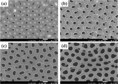
Figure 1 shows the surface FE-SEM micrographs of the AAO template with 0.3 M oxalic acid (H2C2O4) at 70 V, with varying pore-widening times of 10 min, 20 min, 30 min, and 40 min.
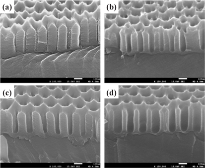
Figure 2 shows cross-sectional FE-SEM micrographs of the AAO template.
Typically, AAO templates have uniform circular holes and a high aspect ratio for use in the preparation of nanotubes or nanowires. However, in this study, the AAO template is used as a chemical sensor to detect various liquid state substances.
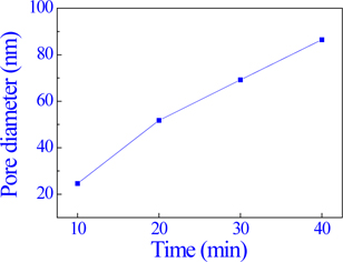
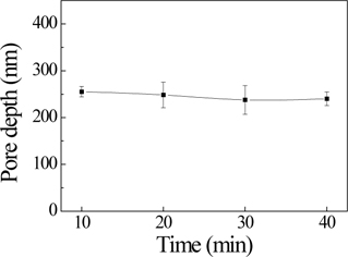
Figure 3 and Fig. 4 show the average pore diameter and pore depth graph, respectively. The average pore diameter increased from approximately 24.6 nm to 86.5 nm with an increase in pore-widening time from 10 min to 40 min. The average pore depth went from being normal to being in the error range as the pore-widening time increased from 10 min to 40 min.
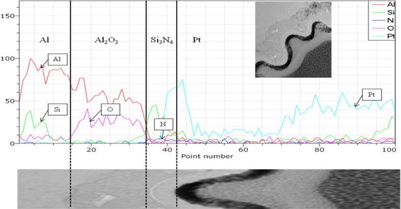
Figure 5 shows a TEM/EDS image of the Si3N4 layer-coated AAO template of approximately 30 nm, in order to observe the formation of the Al2O3 layer with a relatively uniform thickness; diffusion of elements at the interface was not observed. The Si3N4 layer was deposited using the PECVD method.
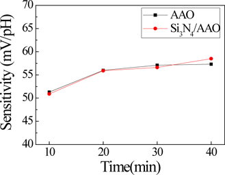
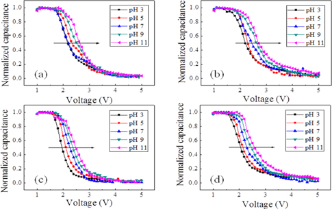
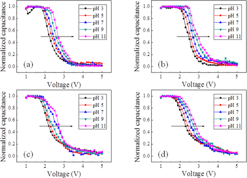
Figure 6 and Fig. 7 show the normalized capacitance-voltage (C-V) characteristics of a single AAO template and Si3N4 layercoated AAO template, respectively. Both Fig. 6 and Fig. 7 seem to display C-V characteristics. Fig. 8 shows that the single AAO template specimen sensitivities are (a) 51.32 mV/pH, (b) 56.00 mV/pH, (c) 57.12 mV/pH, and (d) 57.30 mV/pH. The Si3N4/AAO template specimen sensitivities are (a) 50.90 mV/pH, (b) 55.92 mV/pH, (c) 56.61 mV/pH, and (d) 58.50 mV/pH. These results indicate that sensitivity is not affected. The C-V curves show the detection of ionization by hydrogen ions or hydroxyl ions of the surface hydroxyl groups. The EDM chemical sensor is fabricated using an AAO template as the transducer material. The electrical double layers of the oxide/electrolyte interfaces have been studied extensively [17-19]. C-V measurements were swept from 1 V to 5 V in steps of 100 mV in a linear fashion, which guarantees that only the concentration-dependent potential shift of the resulting chemical sensor is measured. Therefore, the change in the capacitance value at the linear region corresponds to the pH-sensitivity property of the AAO template sensor. It is generally considered that the surface charging mechanism for oxides involves the adsorption of protons or hydroxyl ions by surface hydroxyl groups to form positive or negative sites, respectively.
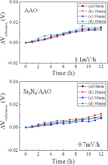
Figure 9 shows the stability drift rate of the AAO template and Si3N4/AAO template with various pore-widening times at a pH of 7. It was observed that the lower the slope of the graph, the more stable the specimen. However, when continuous, it appears to be unreliable because of the physical effects of the strong voltage applied. The reason for the increase in reliability of the Si3N4/AAO template is due to the surface of the template being more stable for a long time because the hardness can be maintained [20]. An Al2O3layer formed on the high voltage quickly forms a soft film, and therefore there is no ambiguity. When depositing Si3N4, it is more stable.
We fabricated an AAO nano template using a two-step anodizing process. In order to increase the stability, Si3N4 was deposited on them using the PECVD method. The AAO template and electrochemical characteristics were observed for application as a chemical sensor. In this study, although the AAO and Si3N4 templates did not display a large difference in terms of sensitivity, the Si3N4 template displayed greater stability and, therefore, appears to have better qualities.