In this paper, we present a submicron patterning method for optical Talbot carpet in a single exposure configuration. We also demonstrate a rigorous simulation for Talbot carpet in nano-scale. In principle, the Talbot carpet originally has an analogy in quantum physics referred to as the “quantum carpet”, which describes the behaviour of localized wave packets, which undergo revivals in time [1]. The Talbot carpets are also found in atomic physics [2], in plasmonics [3, 4], and especially in wave propagation in coherent optics.
Talbot carpet of light is a longitudinal section (in direction of propagation) of the interference pattern behind a 1-dimensional transmission grating illuminated by a coherent plane wave. An image of Talbot carpet contains fractional profiles of a master grating at rational multiples of the Talbot distance. It also contains profiles of fractal Talbot patterns at irrational fractions of the Talbot distance [5-7]. Accordingly, Talbot carpet is highly interesting since the scaling down of feature size is among the critical issues and challenges for submicron to nano-patterning [8, 9].
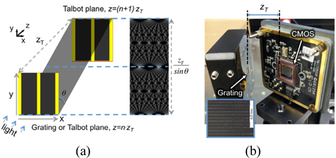
Talbot images or near-field interference patterns behind periodic grating structures were first observed by H. Talbot, who discovered that, at regular distances behind the plane structure, a pattern that replicates the original grating structure is formed [10]. L. Rayleigh explained that the replication distance,
In our interest, the visualization of the optical Talbot carpet is usually performed by computer integration of images recorded by digital camera at different distances from the grating [17-20]. However, in order to obtain the image of the Talbot carpet, a large number of such high-resolution images are required.
Previously, the measurements were done in the visible spectral range and with a large period grating, which made the measurement simpler. Particularly, in the case of submicron gratings, the spatial resolution of optical detectors is not sufficient, so the good way to image the pattern is to record each plane by exposure of photo-sensitive materials such as photoresists [21]. However this is a tedious and time-consuming procedure requiring repeated nano-meter precise positioning of the photoresist plane. Therefore we consider a single exposure imaging method that can record the high-resolution structure of Talbot carpets over a wide range of propagation distances without missing image planes, which can also become a fundamental technique to investigate and utilize the nano Talbot carpets.
In simulation, we study further for a non-paraxial case of Talbot pattern employing finite-difference time-domain (FDTD) simulation by the “Dr Litho” simulator [22, 23]. In this demonstration, extreme ultraviolet (EUV) radiation is used, which can be realized lithographically [24]. We analyse for image properties especially in the rational and irrational intensity profiles in the Talbot carpet. The simulation results show the single exposure configuration for Talbot carpet can produce the ever-decreasing periodicities in nano-scale down to diffraction limit in intensity profiles.
It is well known that the Talbot pattern is a Fresnel image that can be calculated by the angular spectrum representation within Fourier optics [25]. This solution is valid under paraxial approximation when
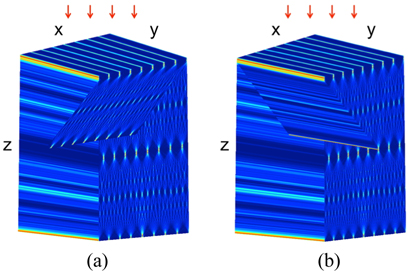
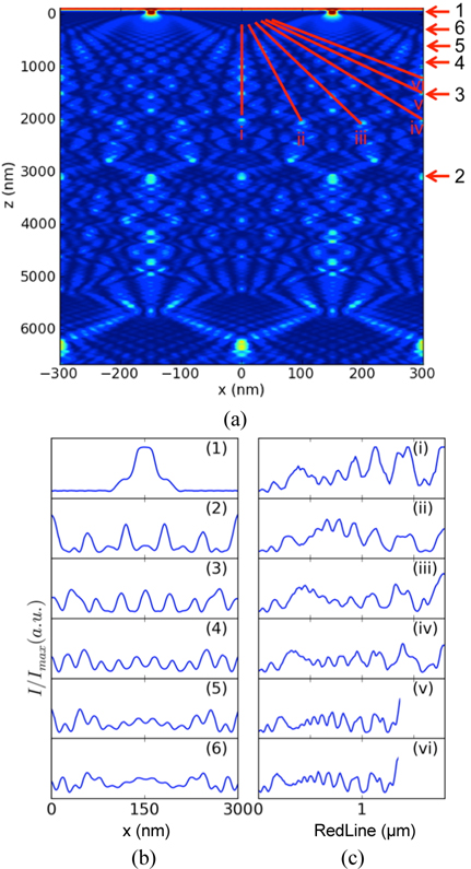
In considering the diagonal cross-sections through the 3-dimensional (3D) image of the Talbot pattern, such a cross-section as shown in Fig. 1(a) shows the Talbot carpet stretched in the z-direction in comparison to the conventional Talbot carpet formed just in the x-z plane. This diagonal cross-section contains the complete Talbot carpet, because all details of the intensity distribution at each z-position are included in those tilted 2D images (diagonal crosssection in Fig. 1(a)). In the space of the Talbot pattern, another diagonal cross-section in Fig. 1(b) is the line-andspace image rather than the traditional Talbot carpet image, which consists of gradually smaller (or bigger) pitches between neighbours.
2.2. Single Exposure Imaging of Talbot Carpet
The method uses a fact that the Talbot carpet is actually located over x-, y-, z-axes, while the conventional method is to scan the profile in the x-axis through the propagation axis as mentioned (see the axis definition in Fig. 2(a)). Here we use diagonal cross-sections in the 3D Talbot pattern to obtain a full image of the Talbot carpet. The object in this case is an ideal binary line-space grating, which is infinitely repeated with a certain period. The object has no variation along the y-axis, and so for the interference image behind the grating, no intensity change exists along the y-axis, while the intensity is modified along the x-axis.
Thus, in the x-y plane at any Talbot distances (
3.1. Experimental Demonstration: Imaging of the Talbot Carpet
In this section, we demonstrate imaging of Talbot carpets in experiments. The exposure was performed with plane wave illumination generated by a highly coherent
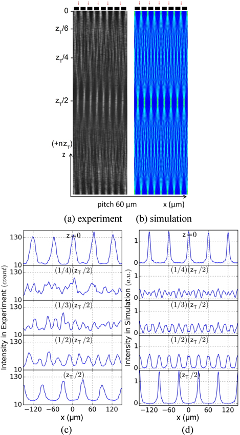
Figure 3(a) shows the result that the Talbot carpet is obtained by the single exposure configuration. The image is recorded in z range between z=zT and z=2・zT, which corresponds to a full Talbot period. The intensity change in center in Fig. 3(a) occurred due to repositioning of the detector that covers a half of the zT (~1 mm).
The resulting image is stretched in propagation direction due to the tilt in comparison to the traditional Talbot carpet formed in the x-z plane. The stretched length (Talbot period) in the tilted plane is magnified by
This method allows characterizing the capability of detectors particularly in terms of resolution. In this demonstration, we used a conventional
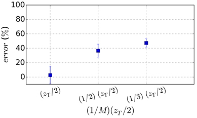
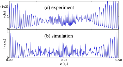
While the Talbot carpet is visualized with a detector positioned perpendicular to the rulings and tilted in the y-z plane as shown in Fig. 1(a) for a horizontal grating, on the other hand, another pattern can be observed with a detector positioned parallel to the rulings and tilted in the x-z plane as shown in Fig. 1(b) for a vertical grating [26]. Such a result obtained in our experiment is presented in Fig. 5(a). The cross-sectional curves (1D profile) of the tilted image (2D image such as a diagonal section in Fig. 1(b)) are displayed in Fig. 5(a) in the range of a half Talbot distance. This profile exhibits various gaps between the peaks through the groove. The gradually increased or decreased gap through the groove is seen in a line-art profile as shown in Fig. 5 for simulation (top) and experiment (bottom), while the profiles of the fractional Talbot pattern show a regular gap as shown in Fig. 3(c, d). The gap (peak to peak) is magnified by (
3.2. Talbot Carpet in Nano-scale: FDTD Simulation
In this section, we demonstrate FDTD simulations with EUV radiation at 13.5 nm wavelength in order to observe the smallest feature in the Talbot carpet. By employing FDTD simulation we can predict the smallest feature in Talbot carpet that will form in the area close to the grating, where the Fresnel-Kirchhoff assumption is not valid. In this regime, the multiple-slits interference influence is reduced but the single slit diffraction features becoming more important. With slit width approaching the wavelength of light the system is entering a non-paraxial regime requiring rigorous calculation. The optical properties of the Talbot image, particularly the intensity, the contrast and the interference fringe quality are dependent on the geometry of the mask and the choice of materials. The large contrast between the transmission of the opening and of the absorber is required and the transmittance has to be optimized with the efficient thickness of the layers for both substrate and absorber in order to obtain the sharper image of the Talbot carpet. For example, in the model we demonstrate for the mask, the pitch was 300 nm, the opening-width was 20 nm and the line-width was 280 nm. The gold is deposited as an absorber layer (60 nm) on Si3N4 membrane (20 nm). This feature is realistic in current mask fabrication technology for EUV radiation [27]. X-ray data for optical properties of materials in [28] were used in the simulation.
Figure 6(a) displays the simulated image of the Talbot carpet behind the grating in the range of
For the case of fractional Talbot pattern as shown Fig. 6(b), spatial frequency is multiplied by up to a factor 15, which results in a corresponding half pitch of 10 nm. The visibility was from 2% at worst and 26% at best. In Fig. 6(c), the fractal Talbot intensity is shown at irrational crosssection as described by Berry [6, 29]. In this case, the width of peaks is decreased along the curves until no peak appears. The contrast is also decreasing as the width decreases and it finally becomes zero at some point, which corresponds to the diffraction limit.
In comparison to conventional methods, the single exposure imaging method enables fast imaging of Talbot carpets, and also depth of focus becomes less critical, because no differential positioning of the detector is required. The experiment can be performed despite the imperfect quality of the grating due to the fact that the Talbot effect reproduces the self-image with modified quality from the grating [30, 31]. This is a well-known effect. However, this is an advantage when applying the method with gratings of smaller pitch.
The single exposure imaging method could be applied for rapid characterization of sources in metrology, where the wave propagation image over near- and far- fields is used for the analysis [20]. The method also enables printing Talbot carpets on photoresist samples using an interference lithography technique. Nano-scale Talbot carpet and fractal Talbot patterning may be feasible utilizing this method.
The rigorous diffraction simulation model has shown that the nano-scale Talbot carpet can be obtained under a coherent extreme ultraviolet radiation. Sub-10 nm scale structures may be realized in this case, while the conventional methods can hardly achieve that. The Talbot effect is valid within the limitation that no evanescent fields are present, and so spatial resolution is limited by diffraction. Thus, a highly efficient diffraction mask and a good coherent illumination exposing large area are required. The standard sample suggested in the FDTD simulation is a good example in this case.
We also suggest that structuring of Talbot carpets can be used for characterization of photoresist. While conventional deep ultraviolet optical lithography meets the demand to continuously shrink device structures, further steps of structure miniaturization can be obtained by EUV lithography [32]. The resolvability of photoresist becomes important in sub-10 nm lithography [21]. Thus this work may be potentially useful for applications of nano-lithography with highly coherent EUV sources [33]. Other possible applications would be nanostructuring of quantum dot arrays, nano-photonic devices, and nano-crystals [34-36].
We present an imaging technique that can perform visualization of Talbot carpets very simply and also precisely. Talbot carpet includes fractional and fractal patterns that feature ever decreasing periodicities in intensity profiles even though a large-scale period in mask is used. The experiment demonstrates that Talbot carpet as a whole can be reproduced in a single exposure configuration. The conventional Talbot carpet and another cross-sectional pattern are visualised with tilted detectors, where the tilting is in the range for detectable angle. It is shown that the method can be applied for resolution characterization of detectors. The method enables characterizing the resolvability of photoresist with high-resolution Talbot image produced by short wavelength radiation. Talbot carpet in nano-scale can be produced with the method introduced here, while conventional methods can hardly achieve this. We utilize FDTD simulations in order to observe the smallest feature of Talbot carpet in non-paraxial condition. Structures down to 10 nm are achieved using a 300 nm pitch mask and 13.5 nm wavelength illumination. It may be feasible structuring of Talbot carpet in nano-scale lithographically as suggested. The method could be potentially useful for characterization of light sources, nano-structuring, or applications in photonic devices.