Organic semiconductors have recently been used as active layers in electronic devices such as field-effect transistors (FETs) [1]. Over the last two decades, organic materials and organic semiconducting devices have become a focus of intense research and advancement in both academia and industry. This significant commercial interest in organic electronics stems from their potential as building blocks for inexpensive and structurally flexible electronic devices, including radio-frequency identification tags, smart cards, light-emitting diodes, and flexible displays [2,3]. For applications involving active circuits, organic field-effect transistors (OFETs) are the devices at the heart of switching and logic operations. The mobility of charger carriers is generally lower than that of crystalline inorganic semi-conductors, thereby limiting switching frequencies and demanding higher voltages for similar current levels. The general electrical characteristics of OFETs are well described within the model of metal-oxide semiconductor FET (MOSFET) theory since the electrical properties of OFETs depend on the properties of the organic layer, such as the active layer material used and the material thickness. Recent improvements to the manufacturing process and modifications of the device structure allow for the fabrication of OFETs with mobility comparable to that of amorphous silicon semiconductors with the former material being a popular choice for the fabrication and performance evaluation of organic thin-film devices [4,5]. Copper phthalocyanine (CuPc) materials are widely used in organic light-emitting diodes (OLEDs) and OFETs. Thus far, considerable experimental effort, such as modification of the film quality, has been devoted to the improvement of the device performance. It is important to understand the electrostatic phenomena at the interface between metal and organic materials in order to improve the organic FET device performance. According to the recent research, it has been revealed little by little that carrier was supplied from source or drain electrode in organic FET. In such situation, understanding of the injection behavior of charges at the metal/organic interface is necessary to improve the organic FET operation. Thus the study of the electrostatic interfacial phenomena in organic FET device, which strongly affects the injection behavior at the organic film and metal interfaces, is of special importance to the fields of organic electronics [3].
In the present paper, we present the current–voltage (I–V) characteristics to clarify that the carrier transport and the threshold voltage were estimated from the I–V curves in CuPc FETs with varying active layer thicknesses and channel lengths. Further, we observed the capacitance–voltage (C–V) properties of a CuPc FET for determining the charge carrier characteristics between an organic layer and an inorganic substrate.
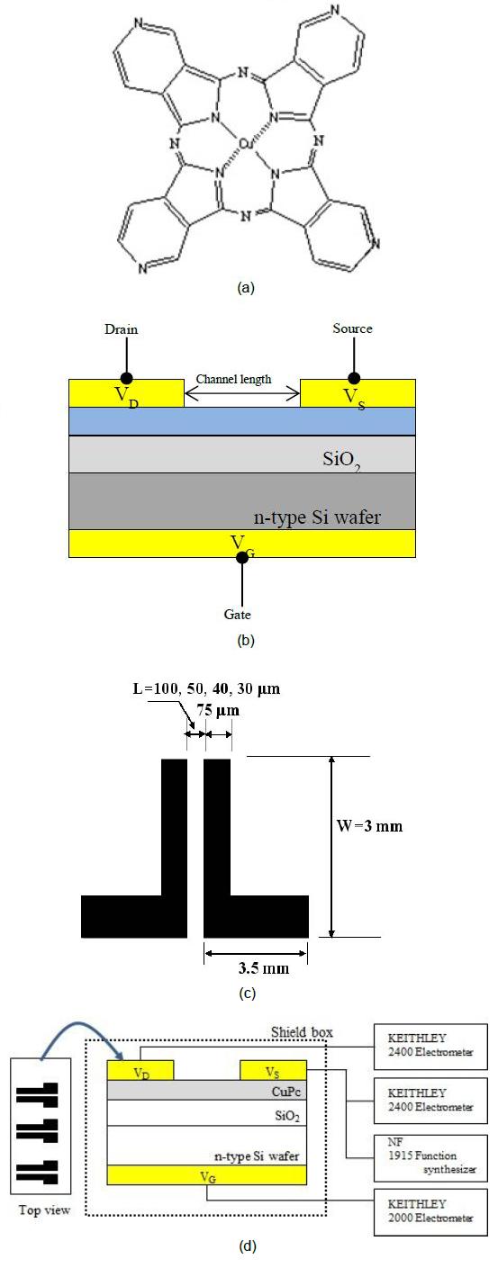
Fig. 1 shows the device structure of a top-contact CuPc FET, the molecular structure of the CuPc materials, and the experimental setup for the measurement of the I–V and C–V characteristics. An Au electrode and a substrate were subjected to an ultraviolet (UV)/ozone treatment on the SiO2 insulating layer for 30 minutes before deposition of the CuPc material and were used a silicon wafer as a substrate.
CuPc was deposited onto the substrate by using the thermal evaporation method at a deposition rate of 0.5 (Å/s) at 10–6 Torr, in various thicknesses such as 5, 10, 20, 40, and 80 nm. Further, the channel length (L) was 30, 40, 50, and 100 mm, and the channel width (W) was fixed at 3 mm. The I–V and C–V measurements were carried out under ambient conditions by using a source meter (Keithley type 2400) and an LCR meter.
In OFET devices, the drive current flowing between the source and the drain,
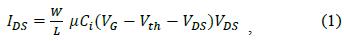
where

In the saturation regime,
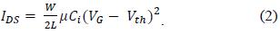
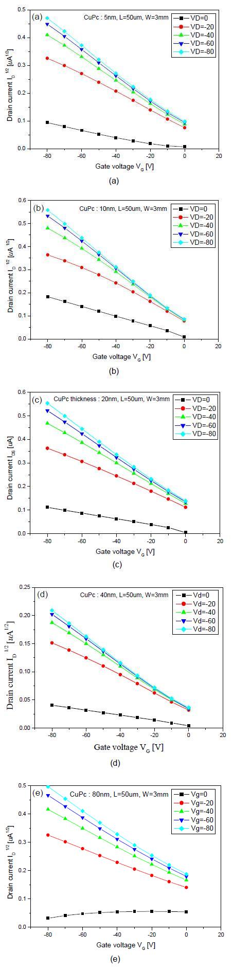
Fig. 2 shows the current–voltage (
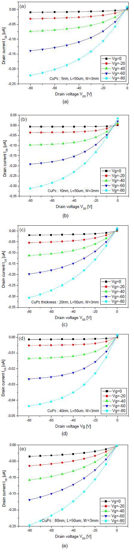
We calculated the carrier mobility of the CuPc FET on the basis of the electrical properties of the CuPc thin films having different active layer thicknesses.
The mobility was 9.7 × 10⁻⁵ cm2V–1s–1, 7.1 × 10⁻⁵ cm2V–s–1, 2.5 × 10⁻⁵ cm2V–1s–1, and 1.2 × 10⁻⁵ cm2V–1s–1 for 5-nm-thick, 20-nm-thick, 40-nm-thick, and 80-nm-thick CuPc FET devices, respectively. The mobility of the CuPc FETs was not very high in comparison with the mobility of pentacene FET, as a reported in references [3,7] (Fig. 3).
From an elementary analysis of
This can be attributed to the fact that the CuPc FET with an active layer thickness of 80 nm did not exhibit sufficient saturation at
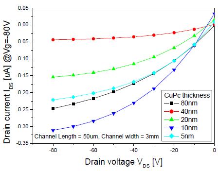
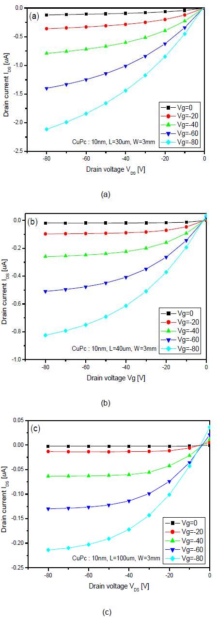
From Fig. 5, we observed that in the 10-nm CuPc FET device, the drain current was higher than that in the other devices. Note that we fabricated CuPc FET devices with different channel lengths of 30, 40, and 100 µm for estimating the electrical characteristics of CuPc FETs.
Fig. 6 shows the I–V characteristics of CuPc FETs with different channel lengths such as 30, 40, and 100 µm. The CuPc FET with a channel length of 40 µm exhibited typical FET characteristics (Fig. 6(c)), and that with a channel length of 100 µm exhibited leakage current at a low drain voltage of less than 10 V. Further, the CuPc FET with a channel length of 30 µm did not have a saturation region at a high drain voltage, as shown in Fig. 6(a).
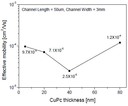
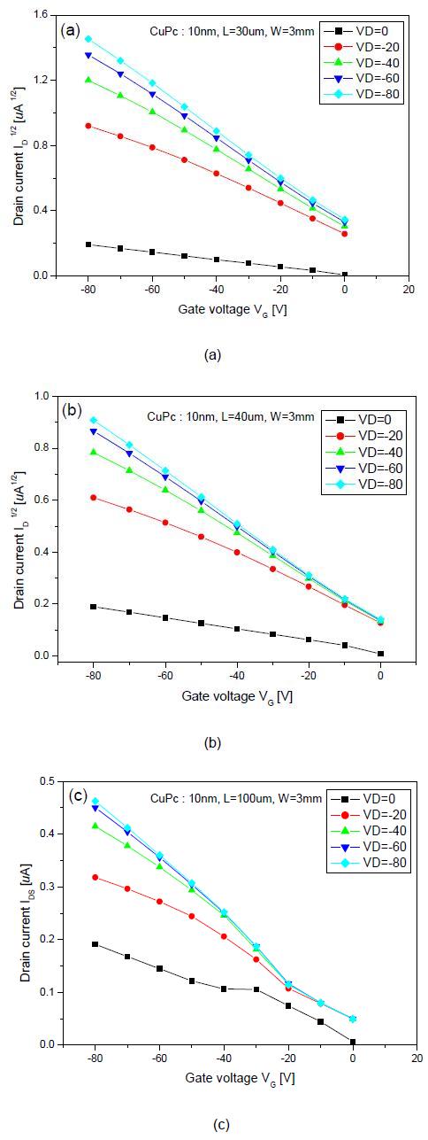
From Fig. 7, we infer that the threshold voltage did not change much for CuPc FETs having different channel lengths. Fig. 8 shows the C–V characteristics of the CuPc FETs, and the bias voltage in the region ranges from –40 V to 40 V at 43 Hz.
From Fig. 8, we infer that the capacitance of the samples increases with an increase in the negative bias voltage and approaches about 97 pF but does not saturate. In this case, the source and the drain electrodes were shorted, and the gate bias voltage
These results were observed for top-contact FETs, and the C–V characteristics can be understood on the basis of a metal-insulator-semiconductor (MIS) capacitor. Further, the difference in the capacitance of the samples with varying channel lengths of the CuPc FETs corresponded to the amount of accumulated carriers at the interface between CuPc and SiO2, which served as an insulating layer [3].
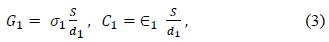
To understand the increase in the capacitance at the interface with bias voltage, the Maxwell–Wagner model was introduced to the top-contact CuPc FET devices.
The ideal image of the Maxwell–Wagner model was explained at the interface such as two dielectric materials in the FET device as shown in Fig. 9. Fig. 9 shows the ideal circuit for this model and the equivalent circuit for double-layered capacitance [3]. The material parameters of each dielectric and the circuit parameters of the equivalent circuit are as follows:


We fabricated the top-contact CuPc FETs with various CuPc thicknesses and different channel lengths. Further, we discussed the transistor properties of these top-contact CuPc FETs, such as the I–V and C–V characteristics. We noted that the increase in capacitance corresponded to the accumulation of carriers at the interface of the metal and CuPc materials.
It is important to understand the electrostatic phenomena at the interface between metal and organic materials in order to improve the organic FET device performance. We confirmed the amount of accumulated carriers as 97 pF at the interface between the CuPc layer and the SiO2 layer from Fig. 8. Further, we calculated that the threshold voltage for varying CuPc thicknesses was about 15–20 V at