검색 전체 메뉴
PDF
맨 위로
OA 학술지
Decimation Chain Modeling for Dual-Band Radio Receiver and Its Operation for Continuous Packet Connectivity
  • 비영리 CC BY-NC
  • 비영리 CC BY-NC
ABSTRACT
Decimation Chain Modeling for Dual-Band Radio Receiver and Its Operation for Continuous Packet Connectivity
KEYWORD
Aliasing , Compressed mode , Continuous packet connectivity , Decimation , Interpolator , Polynomial
  • I. INTRODUCTION

    Decimation is a widely used digital signal processing technique that is employed in various telecommunication fields [1-3]. For a decimation chain to cover multiple bands of cellular telecommunication standards, such as UTRA/FDD, DCS1800, PCS1900, GSM850, and E-GSM900, the chain may bear a polynomial interpolator, which adjusts various sample rates from a multirate oversampling analog-to-digital converter (ADC) to a fixed data rate chosen by the standard under consideration. A good range at the input of the decimation chain is chosen to be more than 289–362 MHz in order to cover multiple bands while the chain finally outputs two sample rates, namely 3.84 MHz and 270.83 kHz, for UTRA/FDD and GSM, respectively. Assuming that the ADC clock (CK) rate is a nominal 312 MHz by default, we find that the oversampling ratio for WCDMA is about 81 with a possible signal-to-noise ratio (SNR) of >70 dB under jitter-free conditions. In turn, an SNR of about 90 dB is attainable for GSM under the same CK rate conditions.

    In this paper, alternative configurations for the decimation chain in multi-standard reconfigurable radios [4-6] are explained and compared from the perspective of covering the 1.9-GHz and 900-MHz frequency bands. The errors incurred by the use of the Lagrange polynomial interpolator are estimated in order to gain insight into the tradeoff between aliasing and the signal bandwidth (BW). Further, the operation of the decimation chain in the compressed mode or a discontinuous transmission is addressed in order to guarantee continuous packet connectivity (CPC).

    II. ALTERNATIVE CONFIGURATIONS FOR THE DECIMATION CHAIN

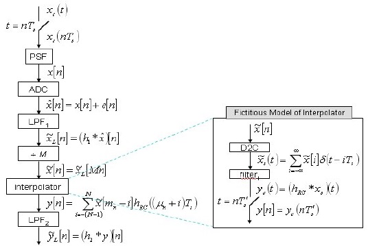
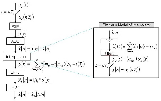
    Two configurations of building-block placement are considered for the decimation chains with data interpolators. Configuration I, shown in Fig. 1, has the interpolator immediately after the ADC, whereas Configuration II, shown in Fig. 2, has the interpolator located after the decimation-by-M (=24) block. Configuration I needs a faster interpolator. The PSF is a pulse shaping filter; here, a root raised cosine filter with a roll-off factor of 0.22 is used for the 1.9-GHz band, while a Gaussian low-pass filter with a normalized BW of 0.5 is used for the 900-MHz band, with no clock jitter assumed. If the roll-off factor drops, the BW becomes more compact. If the normalized BW drops, the intersymbol interference increases but the BW becomes more compact. After a second-order discrete-time delta-sigma ADC is passed, the signal is corrupted with the quantization noise e[n].

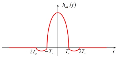
    In Figs. 1 and 2, the interpolator is based on a fictitious model consisting of a discrete-to-continuous (D2C) block and an interpolating filter, filteri, whose impulse response is denoted as hRC [7,8]. The interpolator changes the sample period from Ts to Ts'. Since N is set to 2 in our design, the interpolator is a cubic interpolator. Ideal brick-wall filters are assumed for LPF1 and LPF2 . In practice, the combination of LPF1 and decimation-by-M (÷M) block may be modeled by the cascaded connections of two pairs of a sinc filter and a decimator. A low-pass filter (LPF1 or LPF2 ) is placed after the nonideal interpolator to remove the out-of-channel aliases originating from the interpolator.

    The overall chains in Configuration I shown in Fig. 1 and Configuration II illustrated in Fig. 2 are fed with x[n], a sampled version of xc(t), having a sampling frequency of 1/Ts. xc(t) is assumed to be a non-return-to-zero (NRZ) signal that is pulse shaped by the PSF with the assumption of an ideal wireless channel. For the 1.9-GHz band WDCDMA, the first null of the root raised cosine filter lies at a point about 80 times as large as the sampling period. For the 900-MHz band GSM, a time-domain GMSK pulse is used for pulse shaping and the normalized BW (set to 0.5) results in the intersymbol interference such that the present time symbol overlaps with the next symbol and the previous symbol.

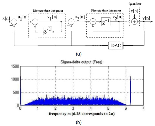
    The delta-sigma ADC in Figs. 1 and 2 is modeled such that the overall noise is e[n] – 2e[n – 1] + e[n – 2] and the theoretical SNR improvement is about 15 dB for every doubling of the oversampling ratio [9]. This ADC is a single-bit second-order discrete-time delta-sigma ADC whose simplified block diagram is shown in Fig. 3(a). The sampling CK rate of the ADC is adjustable to cover multiple bands and modes for UTRA/FDD and GSM.

    A single-tone input near dc, together with random noise, which is calculated from the set SNR and oversampling ratio, is applied at the ADC input. The corresponding spectral-domain output of the ADC is obtained from a simulation and plotted in Fig. 3(b), which exhibits the expected noise shaping behavior of the delta-sigma ADC. A Hanning window is used for obtaining the output power spectral density. Low-pass filters, LPF1 and LPF2 , are modeled as brick-wall filters, and hence, h1[n] and h2[n] are sinc shaped.

    III. POLYNOMIAL INTERPOLATOR AND INTERPOLATION ERROR

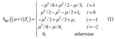
    Configuration I shown in Fig. 1 uses the interpolator to adjust the variable sample rates to 312 MHz, while Configuration II illustrated in Fig. 2 uses it to adjust finally to 13 MHz. The final output sample rates for Configurations I and II are 13 MHz. Among various interpolator types, the Lagrange interpolator is adopted in view of the tradeoff between practicality and performance. From the fictitious model shown in Figs. 1 and 2 and with the introduction of three variables, mn ≡ floor(nTs'/Ts), μn ≡ (nTs'/Ts) – mn (where 0 ≤ μn < 1), and I' = mni [7], the input–output relationship is straightforwardly obtained, where the input is dependent on mn and the interpolating filter hRC is expressed as a polynomial of μn.

    As the summation index N increases, a more accurate interpolation is possible. The value of N is chosen as 2 for practicality [10], which yields a cubic interpolator in terms of μn or μ, as shown in (1). When this hRC(t) is plotted, it manifests itself as a distorted sinc function of a finite duration, as plotted in Fig. 4, whereas a linear interpolating function (when N = 1) appears to have a rectangular shape. If the interpolating filter were a sinc filter, then it would have performed ideal interpolation as expected.

    image

    For various Ts values of interest, both Configurations I and II are compared with the reference configuration, which does not contain an interpolator and uses the default and fixed ADC clock rate of 312 MHz. This newly defined interpolation error (arising from the use of the interpolator) is computed for each Ts by using a new definition (2), where averaging over >100 NRZ bits is performed.

    image

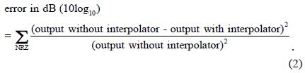
    From a simulation of the process of obtaining the spectrum of this newly introduced interpolation error, we verified that practical polynomial interpolators have aliases that are not of the white noise type but are close to the signal BW. These aliases lead to the interpolation error defined above. From extensive simulations, interpolation errors for various 1/Ts values are computed and plotted in Fig. 5 for both Configurations I and II in the case of the 900-MHz GSM. Similarly, interpolation errors for various 1/Ts values and for both Configurations I and II are plotted in Fig. 6 in the case of the 1.9-GHz UTRA/FDD.

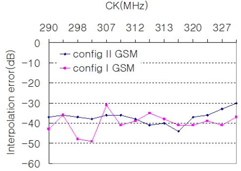
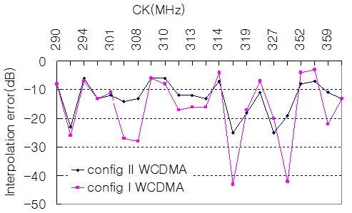
    Thus, we can conclude and verify from the simulated results illustrated in Figs. 5 and 6 that Configuration II exhibits better performance than Configuration I in terms of the variability of the interpolation error over the input sample rates of interest. Furthermore, the following is verified from the simulated results shown in Figs. 5 and 6, on the basis of the newly defined interpolation error: Since the ratio of the sampling frequency to the signal BW for WCDMA is considerably lower than that for GSM, the average interpolation error is significantly larger for WCDMA than for GSM. On the basis of the facts that the variability of the interpolation error is smaller and the operation speed demanded is lower for Configuration II than for Configuration I, Configuration II is chosen to be a better solution; the SNR at its overall output is computed to be more than 30 dB, meeting the SNR requirements of the given cellular standards.

    IV. SELF-TIMING ADJUSTMENT FOR CPC

    The scenario considered in this section is as follows: If the multi-standard multi-band radio receiver based on the multirate ADC and the decimation chain switches its radio access technology or its channel band from one to another, it has to undergo CK-domain crossing if the sample rate of the ADC is directly coupled to the local oscillator (LO) frequency. To guarantee the so-called CPC regarding information transmission, a remedy is needed in the case of the (band) switching mentioned above. In this section, the remedy is accounted for in the context of the compressed mode of operation in WCDMA, but without any loss of generality, it may be applied to discontinuous transmission and reception, idle mode, and slotted mode in other standards as well.

    To guarantee CPC, during the compressed mode of operation, precise timing should not be lost despite the shutdown of the radio transceiver in the mobile device for some time. For WCDMA, precise timing means better than 1/16 of the chip (about 16.276 ns) for 64-QAM. In the case of the compressed mode, the interpolator loses track of the input positions, and the subsequent resetting of the interpolator at the end of the mode will cause some phase error that might be large compared with the error bound dictated by the path searcher or the rake receiver. Since reinitialization of the searcher is known to take more than 100 ms, resetting the path searcher in sync with the interpolator usually causes severe loss of information and hence, throughput degradation. Accordingly, the interpolator should meet the limitation of the sampling phase error or the input timing error imposed by the modem. If the phase error for every CK-domain crossing resulting from the com-pressed mode meets the requirement by the modem, the path searcher can reuse the previously acquired per-finger time delays at the end of the compressed-mode gap, which accomplishes CPC and no throughput loss.

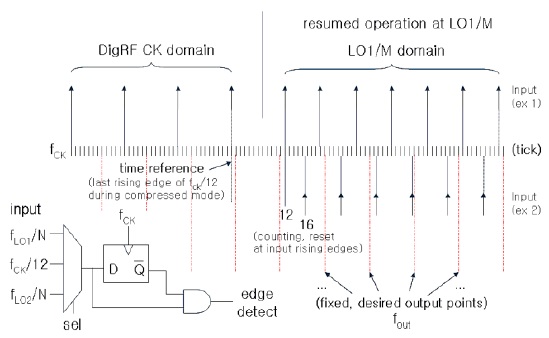
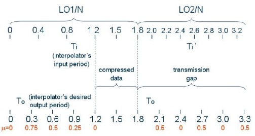
    A simple and practical example of CK-domain crossing caused by the switching from one radio access technology or channel band to another is illustrated in Fig. 7. The interpolator time frame is plotted in Fig. 7 in view of the compressed mode, where Ti (Ti') and To denote the interpolator input and output periods, respectively. Ti and Ti' are directly coupled to the LO frequencies, LO1 and LO2, respectively, through an integer, N. During the compressed mode, the CK domain changes from LO1/N to LO2/N and then, back to the original LO1/N later. Suppose that the LO1/N CK with Ti = 0.4 changes to the LO2/N CK with Ti' = 0.2, owing to the transmission gap, and that the desired target output period of the interpolator, To, is 0.3. The values of μn or μ, defined in Section III, are readily calculated as follows: μ = 0 at To = 0, μ = 0.75 at To = 0.3, μ = 0.5 at To = 0.6, μ = 0.25 at To = 0.9, and μ = 0 again at To = 1.2 in the LO1/N regime. Likewise, the LO2/N regime predicts μ = 0.5, 0, 0.5, 0, and 0.5 at To = 2.1, 2.4, 2.7, 3.0, and 3.3, respectively. In other words, for the output time index k, μ is to be computed for each k by using the equation μ(k + 1) = rem[μ(k) + To/Ti, – 1], where rem denotes the remainder operation.

    The μ values are readily obtained by using an accumulator to update the values periodically. The restarting point of the input samples right after any interrupt interval caused by CK-domain crossing has to be precisely known to facilitate the cross-correlation operation of the path searcher. Just resetting the value to zero at the boundary of the CK transition will result in a random phase or timing error as large as ±0.51/(13 MHz) = ±38.462 ns, which exceeds 1/16 of the chip duration, assuming that the CK frequency lies around 13 MHz (which is the final sample rate after the entire decimation/interpolation).

    A stable and higher-frequency internal CK such as the DigRF CK in the radio chip is utilized to serve as a timing reference and to attain a smooth transition from one CK domain to another. DigRF is the de facto standard for the link interface between the radio chip and the baseband modem chip. In the context of the case shown in Fig. 7, the remedy for CPC is explained as follows: Switch the CK from LO1/N to the DigRF CK before entering the LO2/N CK domain for the compressed mode. This is to resolve the sync issue during the settling of the LO phase-locked loop to a new frequency, which may usually take >100 μs. The switching shall be synchronized to a submultiple of the LO1/N CK edge to meet the sampling phase error mandated by the path searcher. During the DigRF CK mode, the interpolator updates the values of μ with the appropriate To/Ti at the DigRF CK frequency or its submultiple. When the LO2/N CK is stable, the CK switches from the DigRF CK domain to LO2/N. Now, the switching shall be synchronized to a submultiple of the LO2/N CK edge and the value of μ is correspondingly updated. The DigRF CK combined with an edge detector is employed as a position reference, and this reference together with a counter counts and resets some edges across the boundaries of the CK-domain crossing, to the degree of accuracy mandated by the rake receiver. The error after every switching will be about one DigRF CK cycle, which suffices for the modem operation without having to reinitialize the searcher.

    A simple method to detect the sample phase error at a clock boundary by using a CK at a high frequency, fCK, is illustrated in Fig. 8, where the LO1/M domain is resumed after the compressed mode (Here, M is merely an integer.). To know the correct input sample time points, for example, either ex 1 or ex 2 in Fig. 8, after the CK-domain crossing boundary, an edge detector and a counter are employed at the fCK rate. In the DigRF CK domain, the fCK/12-rate input samples are edge-detected at the fCK rate and the counter at the fCK rate counts from a rising edge of the input sample to the next rising edge and is immediately reset. As shown in Fig. 8, for input ex 1, the counter is reset to zero at 12, while for input ex 2, the counter is reset to zero at 16.

    If the data are in the LO1/M domain, then the fLO1/N-rate input samples are chosen by the control input, sel, of the multiplexer, and thus, their edges are detected. Thus, self-timing adjustment can be attained through the use of a high-frequency CK, such as in DigRF, at fCK. This remedy for CPC was tested on a multi-band multi-standard radio transceiver and was proven valid for a crossing of sampling CK from 289 MHz to 337 MHz and vice versa, controlled by the 312-MHz DigRF CK. The edge detector and the counter may be merged and implemented as a time-to-digital converter as another option [11].

    V. CONCLUSION

    Decimation chain structures for dual-band radio receivers are modeled, and two alternative configurations are analyzed in terms of signal BW and aliasing. With the introduction of a new criterion, the interpolation error, the performances of the alternative configurations are analyzed and compared for both 1.9-GHz UTRA/FDD and 900-MHz GSM bands, which provides insight into the origin of aliases and the tradeoff between aliasing and signal BW. Each configuration is modeled with a cubic Lagrange interpolator in conjunction with a multirate delta-sigma ADC, targeted for a multi-standard multi-band reconfigurable radio. The sample rate processor is further extended to cover the issue of inter-radio-technology or inter-channel switching, which gives rise to CK-domain crossing. A remedy is proposed to deal with this issue, thereby maintaining CPC in the compressed mode of operation in WCDMA and in practically equivalent modes in other standards.

참고문헌
  • 1. White B. A., Elmasry M. I. 2000 "Low-power design of decimation filters for a digital IF receiver," [IEEE Transactions on Very Large Scale Integration (VLSI) Systems] Vol.8 P.339-345 google cross ref
  • 2. Chang H. M., Yang J. S., Lee W. C. 2011 "Low-latency digital-IF scheme using an IIR polyphase filter structure for delay-sensitive repeater systems," [IEICE Transactions on Fundamentals of Electronics, Communications, and Computer Sciences] Vol.94A P.1715-1723 google cross ref
  • 3. Kim M., Moteki T., Ichige K., Arai H. 2009 "Efficient heterodyne digital receiver with direct RF-to-digital conversion for software defined radio," [IEICE Transactions on Fundamentals of Electronics, Communications, and Computer Sciences] Vol.92A P.1056-1062 google cross ref
  • 4. Hueber G., Stuhlberger R., Springer A. 2008 "An adaptive digital front-end for multimode wireless receivers," [IEEE Transactions on Circuits and Systems II: Express Briefs] Vol.55 P.349-353 google cross ref
  • 5. Uusikartano R., Takala J. 2004 "A low-power fractional decimator architecture for an IF-sampling dual-mode receiver," [in Proceedings of the International Symposium on Circuits and Systems (ISCAS’04)] P.589-592 google
  • 6. Shahana T. K., Jose B. R., Jacob K. P., Sasi S. 2009 "Decimation filter design toolbox for multi-standard wireless transceivers using MATLAB," [International Journal of Signal Processing] Vol.5 P.154-163 google
  • 7. Gardner F. M. 1993 "Interpolation in digital modems. Part I: Fundamentals," [IEEE Transactions on Communications] Vol.41 P.501-507 google cross ref
  • 8. Erup L., Gardner F. M., Harris R. A. 1993 "Interpolation in digital modems. Part II: Implementation and performance," [IEEE Transactions on Communications] Vol.41 P.998-1008 google cross ref
  • 9. Aziz P. M., Sorensen H. V., van der Spiegel J. 1996 "An overview of sigma-delta converters," [IEEE Signal Processing Magazine] Vol.13 P.61-84 google cross ref
  • 10. Meyr H., Moeneclaey M., Fechtel S. A. 1998 Digital Communi-cation Receivers. P.505-532 google
  • 11. Ramakrishnan V., Balsara P. T. 2006 "A wide-range, high-resolution, compact, CMOS time to digital converter," [in Proceedings of the 19th International Conference on VLSI Design] google
이미지 / 테이블
  • [ Fig. 1. ]  Configuration I where the interpolator is placed immediately after the analog-to-digital converter (ADC). PSF: pulse shaping filter, LPF: low-pass filter, D2C: discrete-to-continuous.
    Configuration I where the interpolator is placed immediately after the analog-to-digital converter (ADC). PSF: pulse shaping filter, LPF: low-pass filter, D2C: discrete-to-continuous.
  • [ Fig. 2. ]  Configuration II where the interpolator is placed after the decimator. PSF: pulse shaping filter, ADC: analog-to-digital converter, LPF: low-pass filter, D2C: discrete-to-continuous.
    Configuration II where the interpolator is placed after the decimator. PSF: pulse shaping filter, ADC: analog-to-digital converter, LPF: low-pass filter, D2C: discrete-to-continuous.
  • [ Fig. 3. ]  (a) Simplified block diagram of a second-order discrete-time delta-sigma analog-to-digital converter (ADC). (b) Output power spectral density of the delta-sigma ADC in case a single-tone signal plus noise is applied at the input.
    (a) Simplified block diagram of a second-order discrete-time delta-sigma analog-to-digital converter (ADC). (b) Output power spectral density of the delta-sigma ADC in case a single-tone signal plus noise is applied at the input.
  • [ ] 
  • [ Fig. 4. ]  Impulse response of the cubic Lagrange interpolator.
    Impulse response of the cubic Lagrange interpolator.
  • [ ] 
  • [ Fig. 5. ]  Interpolation errors of Configurations I and II in the case of the 900-MHz band (GSM).
    Interpolation errors of Configurations I and II in the case of the 900-MHz band (GSM).
  • [ Fig. 6. ]  Interpolation errors of Configurations I and II in the case of the 1.9-GHz band (UTRA/FDD).
    Interpolation errors of Configurations I and II in the case of the 1.9-GHz band (UTRA/FDD).
  • [ Fig. 7. ]  Time frame for interpolator operation in the compressed mode.
    Time frame for interpolator operation in the compressed mode.
  • [ Fig. 8. ]  Method to identify correct input sample points of the interpolator at a clock (CK) boundary.
    Method to identify correct input sample points of the interpolator at a clock (CK) boundary.
(우)06579 서울시 서초구 반포대로 201(반포동)
Tel. 02-537-6389 | Fax. 02-590-0571 | 문의 : oak2014@korea.kr
Copyright(c) National Library of Korea. All rights reserved.