Electronic warfare support measures (ESM) systems are required to generate an electronic order of battle. For his purpose, an ESM receiver must intercept emissions from all nearby radars, and measure parameters such as frequency, time-of-arrival, and angle-of-arrival [1].
ESM for electronic intelligence (ELINT) applications places stringent demands on a receiver over a multi-octave bandwidth. Practical solutions must not only meet the electrical specifications but also be compact and immune to microphonic effects and thermal fluctuations. A wideband receiver module was designed to meet these requirements and to provide matching phase and amplitude [2]. A wideband receiver that is located next to an antenna requires low noise figures (NFs) because very low input signals are received by the antenna.
Unfortunately, a low-noise amplifier (LNA) is limited to NF characteristics. Studies have attempted to overcome this limitation by combining two channels. In this case, phase matching between two channels is very important because it can affect the NF.
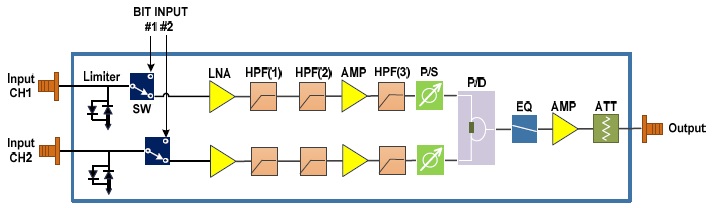
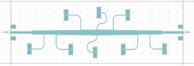
Fig. 1 shows the block diagram of a wideband receiver with two input channels and one output channel.
A limiter, located in the first stage, is used to protect the receiver module against a high power input signal. If the components in the receiver module are damaged, the module will not operate. A switch between the limiter and the LNA can select the radiofrequency (RF) path or built-in test (BIT) path that might be used for calibration. A high-pass filter (HPF) is used to eliminate undesirable input signals from the bandwidth. A power combiner is used to combine the two input signals to improve the NF. The phase shifter is for beamforming.
Compared with other receivers, the proposed wideband receiver performs better in terms of NF and phase matching between ports. It was fabricated from 5-mil RT5880 and 10-mil alumina material with gold plating, which can easily be assembled using gap weld bonding.
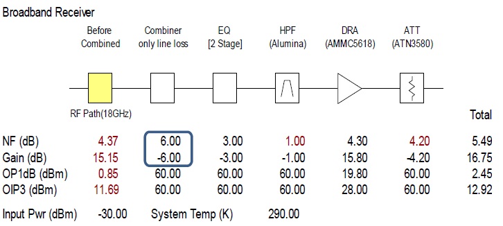
To satisfy a system’s requirements for the broadband receiver to be located in the front end behind the antenna, the NF, linear equalizer, power divider, and HPF have been considered in the design.
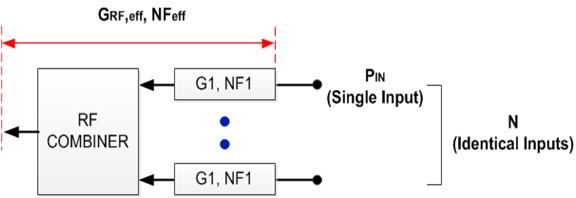
To reduce the NF, a power combiner can be used to combine two input channels. Fig. 2 shows a block diagram for N input signals; the NF can be calculated using Eq. (1). The effective gain (
If there was perfect impedance matching in the combiner cascade, any mismatches would result in a loss of power that would be dissipated in the combiner network.

Using Eq. (1), the effective NF (
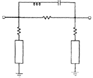
As shown in Figs. 3 and 4, if a transmission line with a serial resistor is open at a frequency equivalent to the resonance frequency of the inductor and capacitor, the insertion loss ideally becomes zero. The rest of the band is designed to undergo attenuation owing to the T-network of the three resistors, which determines the slope of the line [4].
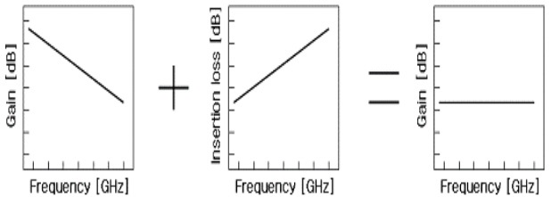
The broadband receiver tends to end up with increasing overall insertion loss that is attributed to the cascaded placement of dissipative components such as the switch, filter, power divider, and coupler in the wide band RF channel. To achieve the desired quality performance, it is necessary to compensate for the insertion loss with flattening in the gain amplitude over the frequency band of interest. This produced uniform gain performance. The equalizer flattened the amplitude of the resultant insertion loss of the equalizer following the former component over the specified band [5].
3. Broadband Wilkinson Power Divider
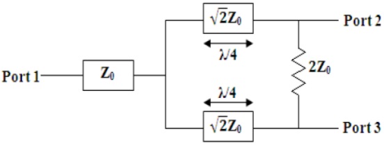
The transmission line modeling (TLM) of a two-way equal split Wilkinson power divider (WPD) is shown in Fig. 5. This power divider contains one input port, two quarter-wave transmission lines, two output ports, and one isolation resistor across the output ports.
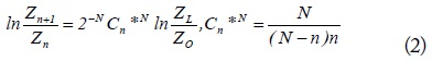
To increase the bandwidth of the input and output responses of the power divider, a binomial multisection matching transformer is used to minimize the ripple levels. To determine the characteristic impedance, Zn+1 of the multisection, beginning with

where
A spurious tone is very important because it a negatively influences signal processing in the total system when unwanted signals come into a broadband receiver. If a spurious tone affects the RF input at low frequency, it creates a harmonic frequency within the operating bandwidth. An HPF is necessary to cancel the spurious tone.
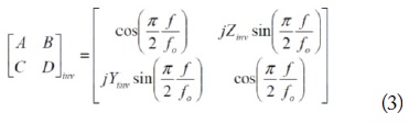
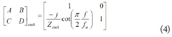
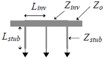
An HPF can be designed as a band-pass filter (BPF) where possible. For the HPF shown in Fig. 6, the ABCD parameters of the impedance inverters and stubs are given by Eqs. (3) and (4), where
The stub length is determined by choosing
The design data of the stub admittances for a maximally flat response can be found where


The design of the broadband receiver should consider the NF, linear equalizer, power divider, and HPF. The receiver should have the same width to connect different materials and to prevent mismatch. The fabrication is based on the width of the microstrip line of an alumina PCB matched with a microstrip line of a 5-mil RT5880 substrate (
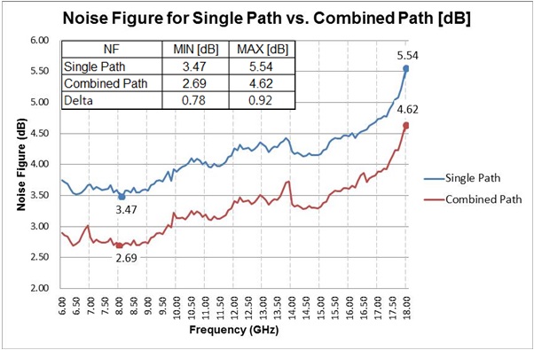
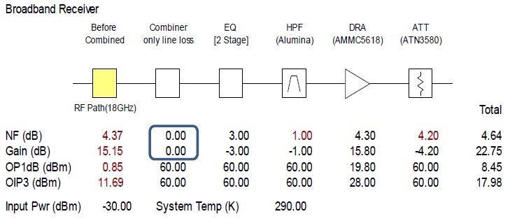
In the combined configuration, the NF was calculated using Eqs. (1) and (2). The combined NF could be improved by approximately 0.85 dB over the NF in a single path. Tables 1 and 2 show how the NF changes in terms of the input signal through a single or combined path.
[Table 1.] Noise figure budget analysis for single path
Noise figure budget analysis for single path
[Table 2.] Noise figure budget analysis for combined path
Noise figure budget analysis for combined path
Fig. 7 is based on a PCB material having a dielectric constant of 9.8 and a 10-mil alumina substrate including a thin film resistor (TFR) to reduce the size of the two stages. A 6-18 GHz super-broadband microstrip equalizer was designed according to the resonance and transmission line theory. The transmission line with a serial microstrip line was opened at a frequency equivalent to the resonance frequency (λ/4).
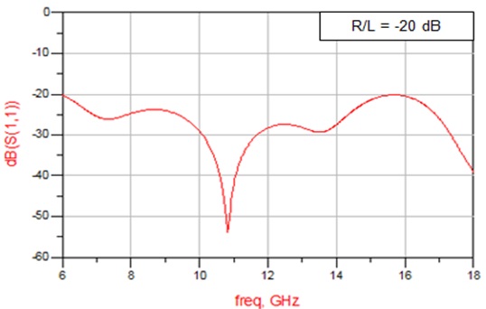
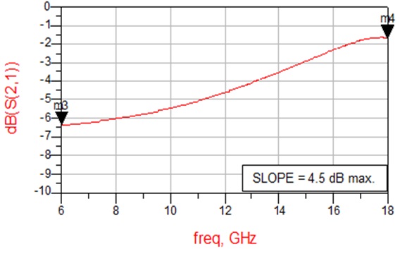
Figs. 8 and 9 show that the input reflection coefficient is a maximum of -20 dB and the amplitude slope is approximately 4.5 dB. The slightly nonlinear behavior seen at 18 GHz arises from the parasitic capacitance of the TFR and transmission lines.
3. Broadband Wilkinson Power Divider
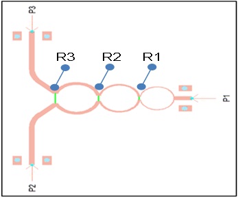
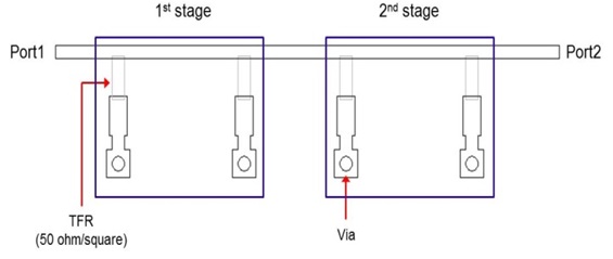
The geometry of a three-stage WPD with in microstrip configuration is shown in Fig. 10. P1 is used to feed the linear equalizer, and P2 and P3 connect RF channels 1 and 2 by gap weld bonding.
A PCB material with a dielectric constant of 9.8 was used with a 10-mil alumina substrate including a TFR that comprised three stages. The characteristic impedance of the λ/4 line at the center frequency of 12 GHz is determined using Eq. (2), where R1, R2, and R3 are the isolation resistors of the multisections as shown in Table 3.
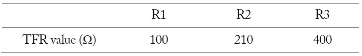
[Table 3.] Resistor values of three-stage Wilkinson power divider

Resistor values of three-stage Wilkinson power divider
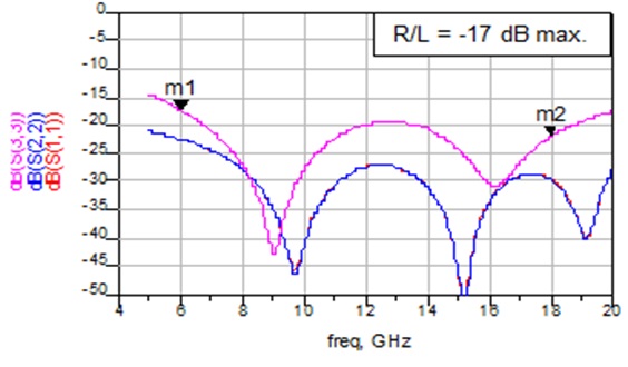
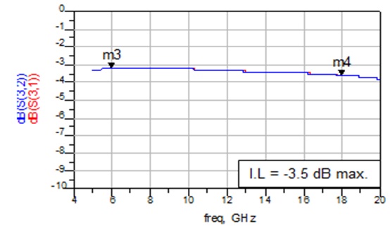
Fig. 11 shows that the input reflection coefficient at each port is a maximum of -17 dB, and Fig. 12 shows that the insertion loss is about around -3.5 dB.
The HPF shows a periodic response owing to its distributive nature. It acts as a BPF from DC to 2
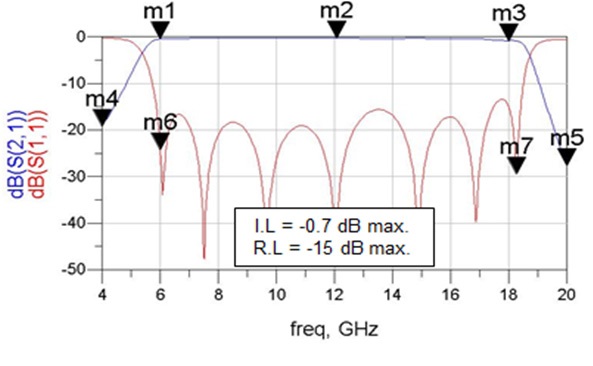
Fig. 14 shows the performance over a bandwidth where the return loss is -15 dB and the insertion loss is -0.7 dB over 6–18 GHz. The rejection value at 4 GHz is around -18 dB and it can be assumed to be -54 dB after cascading over three HPFs.
IV. FABRICATION AND MEASUREMENT
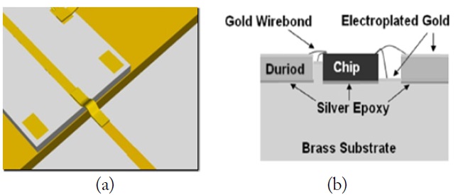
A GaAs MMIC chip was mounted on a gold-plated substrate to provide good grounding. A high-frequency Duroid PCB was placed around the chip to connect the DC bias, and input and output lines were wire bonded.
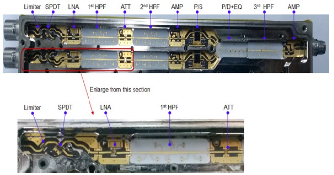
Special attention was paid to minimize the length of the wire bonds at the RF signal and ground line [7]. The manufactured wideband receiver comprised a limiter, HPF, power combiner, equalizer, and amplifier. Fig. 15 shows the fabricated module of the broadband receiver with two input channels and one output channel.
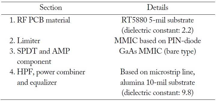
Table 4 summarizes the materials used in the receiver. The length of the wire bond needs to be considered when assembling the receiver to ensure phase matching.
[Table 4.] PCB and active component lists

PCB and active component lists
Fig. 16(a) and (b) show how different PCBs are connected using gap weld bonding and the MMIC chip and Duroid substrate, by wire bonding.
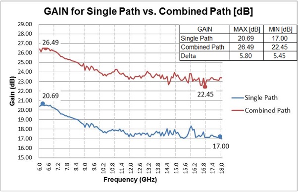
Figs. 17 and 18 show the measured gain and noise figure in a single path. The gain is more than 17 dB and, the NF improves to a maximum of 5.54 dB in the 6–18 GHz band, respectively. In comparison with the simulated and measured result based on Table 1 and Fig. 18 in the single path, the measured result is approximately equal to the simulated result, being difference by only 0.05 dB.
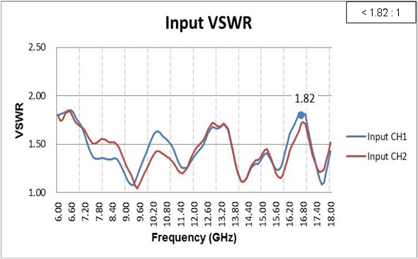
A combined noise figure can be calculated using Eq. (1). The NF is approximately 0.78 dB less than that for a single path. A voltage standing wave ratio (VSWR) for the input of each port is shown in Fig. 19. The results are less than 1.82:1 over the 6–18 GHz bandwidth.
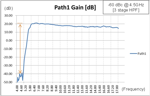
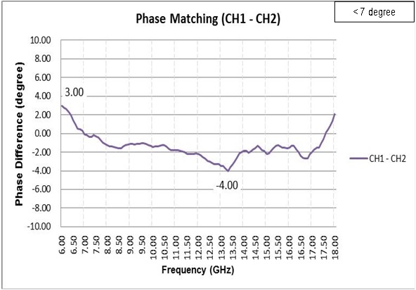
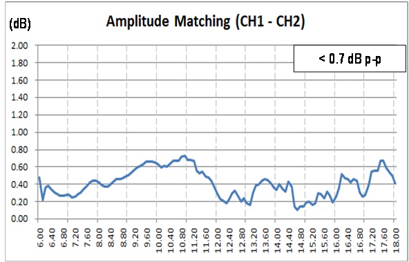
The rejection value for 4.5 GHz in the module is approximately 60 dB after cascading through three HPFs, as shown in Fig. 20. An HPF was designed to reject undesirable spurious tones at low frequency. Fig. 21 shows the value of phase matching (7°), and Fig. 22 shows the value of amplitude matching (0.7 dB p-p).
Figs. 21 and 22 prove that the components were operating properly and that the same bonding length, for both wire bonding and gap welding, was used in each RF channel.
This paper proposes a 6–18 GHz front-end broadband receiver module with two input channels and one output channel. This high-performance broadband receiver has low NF and good phase matching, making it ideal for ESM applications. A broadband receiver based on a combined configuration can be used to achieve low NF.
We conclude that our receiver module significantly improves the noise figure by as much as 0.78 dB over the measured data with a maximum value of 5.54 dB over the 6–18 GHz bandwidth. In addition, the difference value of phase matching is within 7° between ports.
In the future, this receiver module could be implemented for ESM applications to improve the NF and phase matching performance.