An impedance transformer (IT) is one of the fundamental components in RF and microwave circuits. It transforms a specific impedance to another impedance and has been implemented in various applications, such as power dividers [1], baluns [2,3], and antennas [4]. In [5], an open-circuited coupled line impedance transforming symmetric Chebyshev and asymmetric Butterworth DC blocks were presented. It can provide a perfect matching performance at a center frequency (f0) with a relatively narrow bandwidth. Similarly, a multi-conductor coupled transmission line (TL) was proposed in [6], in which the coupled port was connected back to the input port in order to enhance the bandwidth. However, the out-of-band suppression is poor. The IT using a lumped equivalent circuit of left-handed TL section with an impedance transforming ratio (r) of 2 was mentioned in [7]. All presented works were focused on the passband matching characteristics only and did not consider an out-of-band suppression characteristic. If a frequency selective IT can be realized, the total size, insertion loss, and out-of-band suppression of the RF circuit or system can be improved. To enhance the out-of-band suppression with the bandpass response, coupled TLs IT with shunt TL were proposed in [8,9]. Moreover, an ultra-high impedance transforming ratio IT was designed using two cascaded coupled TLs [10]. There are three different matching regions which are categorized by different performances. However, the presented works did not provide a high frequency selectivity characteristic. In [11], the high frequency-selectivity impedance transformer was presented using coupled TL and shunt step impedance transmission lines. The transmission zero can be controlled by varying characteristic impedances of shunt TLs. However, the variation of transmission zero is limited due to the realization of high and low characteristic impedance TLs of shunt stub TL.
In this paper, a design method for an IT with high selectivity characteristics is presented based on parallel coupled TLs. The characteristic impedance of a shunt coupled TL can be provided with wideband and high selectivity characteristics. To verify the proposed IT network, a 50- to 20-Ω IT was designed, simulated, and fabricated at the f0 of 2.6 GHz.
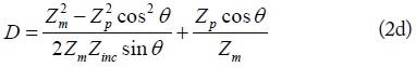
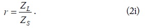
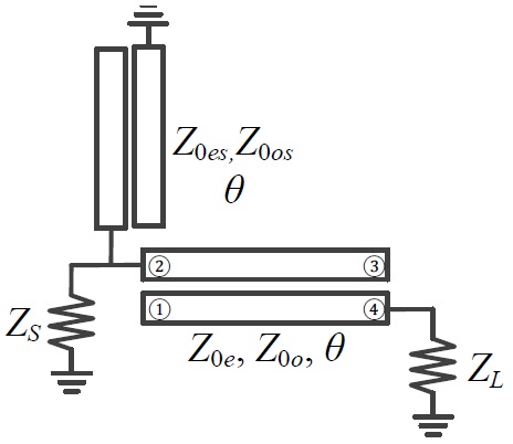
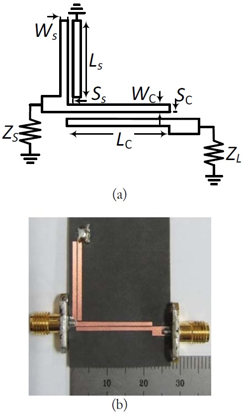
Fig. 1 shows the proposed IT structure. It consists of a series coupled TL with odd- and even-mode impedances (Z0o and Z0e) and a shunt coupled TL with odd- and even-mode impedance (Z0os and Z0es) connected at the source impedance. The electrical length (θ) of both coupled TLs is given as the quarter-wavelength (λ/4) at f0. The load impedance (ZL) can be transformed to the source impedance (ZS) by controlling Z0o and Z0e of the series coupled TL. Moreover, the shunt coupled TL is used to create passband transmission poles as well as two transmission zeros near to the passband, which are located at the lower and upper sides of the passband, respectively.
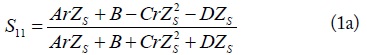
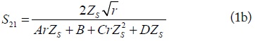
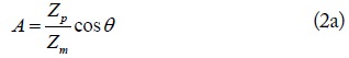
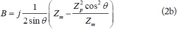
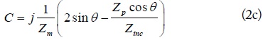
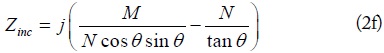
The reflection and transmission coefficients of the proposed IT network can be derived from [12], as shown in Eqs. (1) and (2)
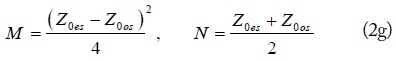
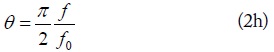
where
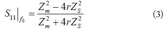
At f0, the reflection coefficients can be reduced as (3).
As seen from this equation, the reflection coefficient only depends on Z0e and Z0o of the series coupled line, and is independent of Z0es and Z0os.
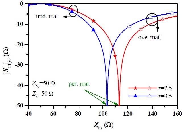
Using (3), the calculated reflection coefficient (S11) at f0 according to Z0e is shown in Fig. 2 by assuming Z0o = 50 Ω, ZL = 50 Ω, ZS = 20 Ω and 14.3 Ω (r = 2.5 and 3.5). From Fig. 2, the reflection coefficient can be categorized into three different matching regions [8] depending on Z0e, which can be described by (4).
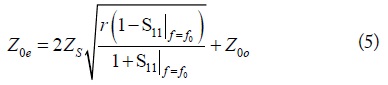
The value of Z0e with specified values of S11, ZS, and r at f0 can be found by using (3) and (4a) for an under-matched region, as shown in (5).
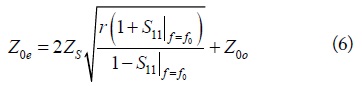
Similarly, the value of Z0e for an over-matched region can be found from (3) and (4b), as shown in (6).
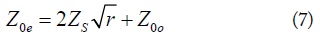
For the perfect matched region, S11 becomes zero. Therefore, the value of Z0e can be determined as (7).
As seen from (5), (6), and (7), characteristic impedances (Z0e, Z0o) of a series coupled TL can be controlled bythe return loss and r. In addition, characteristic impedances of the shunt coupled TL are determine to provide transmission poles in the passband and transmission zeros in the out-of-band.
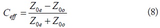
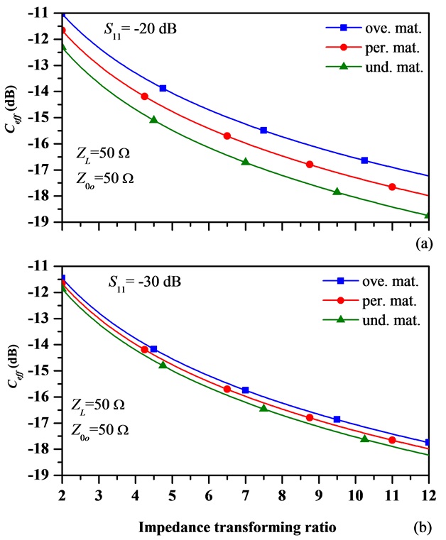
From (5), (6), and (7), the coupling coefficient (Ceff) of series coupled line for different matched regions are obtained as (8).
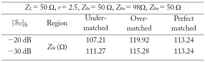
The calculated coupling coefficients of series coupled line are plotted in Fig. 3 according to different r, matched regions, and return losses. The calculation is done by assuming ZL = 50 Ω, Z0o = 50 Ω, and S11 = -20 dB and -30 dB. The calculated values are also shown in Table 1 for different return losses and matched regions. As seen from Fig. 3, Ceff decrease as r increases. Therefore, the series coupled TL can be easily realized for high r without any fabrication difficulty. Also, a high return loss characteristic can be achieved using a loose Ceff.
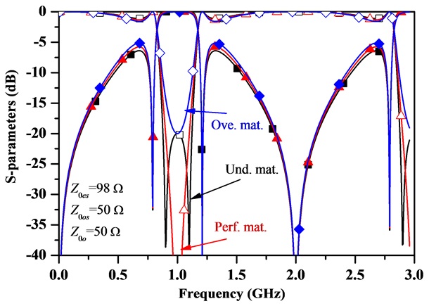
To verify the analytical design equations, the S-parameter characteristics are shown in Fig. 4 for the maximum S11 of -20 dB in the case of the under-matched, perfect matched, and over-matched regions. As seen from Fig. 4, two poles in passband are obtained only in the case of the under-matched region, whereas a single pole is obtained in the perfect matched and over-matched regions. Therefore, the under-matched region is preferable for the widest return bandwidth characteristics.
By choosing Z0es = 98 Ω and Z0os = 50 Ω, the transmission zeros are located at the same frequency for all matched regions.
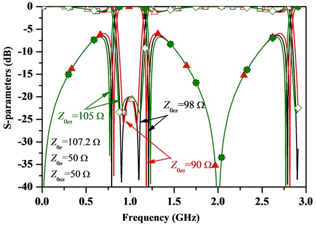
Fig. 5 shows S-parameter characteristics in the undermatched region with different even-mode impedances of shunt coupled TL for investigating selectivity and transmission poles. As Z0es decreases, the transmission poles are moved to near the passband which provides a good frequency selectivity characteristic. However, the bandwidth of the passband is slightly narrowed with smaller Z0es. Therefore, the trade-off between the bandwidth and frequency selectivity characteristic is required to choose a proper Z0es.
For validation of the proposed IT network, the 50- to 20-Ω (r = 2.5) IT with the maximum S11 of -20 dB at 2.6 GHz was designed, simulated, and measured. According to the simulation performance shown in Fig. 4, the under-matched region was chosen. The circuit was fabricated on an RT5880 substrate with εr = 2.2 and h = 31 mil. The electromagnetics (EM) simulation was performed using HFSS v15 from Ansoft.
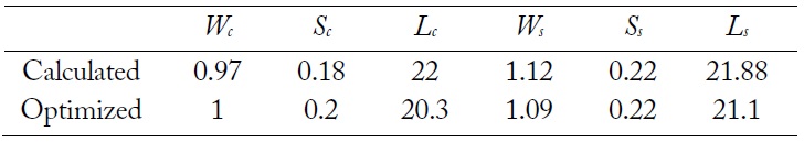
The circuit size of the proposed IT is 27 mm × 30 mm. Fig. 6 shows the EM simulation layout and photograph of the designed IT network. The calculated and optimized physical dimensions are shown in Table 2.
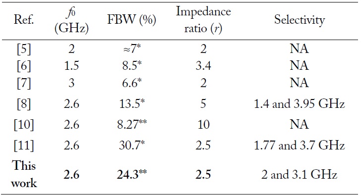
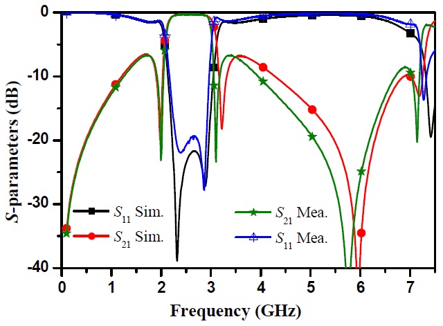
Fig. 7 shows the EM simulation and measurement results of the fabricated circuit. The measured results are in good agreement with the simulations. From the measured results, the return loss was determined to be 19.6 dB at f0. Similarly, 19 dB return loss bandwidth is 0.63 GHz (2.28–2.91 GHz). The maximum insertion loss in the same passband is smaller than 0.4 dB. As seen from the measurement result, one transmission zero is obtained on the lower side near the passband and three transmission zeros are on the upper side, providing good selectivity characteristics. A λ/4 shunt coupled TL generates three transmission zeros at 2 GHz, 3.1 GHz, and 7.14 GHz, respectively. Moreover, the λ/4 series coupled TL generates a transmission zero at 5.75 GHz. The proposed IT provides sharp frequency selective matching and out-of-band suppression characteristics. The selectivity characteristic of the proposed IT is beneficial when it is applied to frequency selective circuit designs, such as high power, high efficiency, and high linear amplifier designs. The performance comparisons with previous published works are summarized in Table 3. Although reference [11] provides a wider fractional bandwidth (FBW), the selectivity is worse than the proposed circuit.
This paper presents the design of an impedance transformer with frequency selectivity characteristics. The frequency selective characteristic can be controlled by changing the shunt evenmode impedances of the shunt coupled transmission line. Both the simulation and measurement results were provided to validate the proposed impedance transformer. The proposed impedance transformer is simple to design and fabricate in the microstrip line.