Since the seminal work reported by Yablonovitch [1] in 1987, photonic crystals [2, 3] have attracted considerable research interest in various fields of study. Photonic crystals are artificial structures in which different dielectric materials are arranged to form periodically varying dielectric constants throughout the structures. It has been demonstrated that photonic crystals are capable of generating, manipulating, and detecting electromagnetic waves [3]. Such artificially created periodically arranged photonic crystals show many unique phenomena that cannot be seen in conventional natural materials. Some of these unique phenomena include negative refraction [4, 5], super-lensing [6, 7], super-prism [8, 9], sharply bent waveguide [10], and slow light [11]. Many theoretical and experimental works have been carried out by numerous investigators to study these unique phenomena and apply these phenomena to a variety of unique applications.
In the past two decades or so, light-emitting diodes have become an essential technology for a variety of display applications, and their application has been extended to general indoor and outdoor lighting as well [12, 13] due to their small size, long life, and high efficiency. However, high light extraction efficiency is desirable as the light emitted from LEDs has a tendency to propagate in any direction. An appropriately designed photonic crystal can function as a photonic insulator for a designated polarization and wavelength range of light. This characteristic of photonic crystals can be applied to enhance the light intensity in certain directions. There have been several investigations to enhance the light extraction of LEDs by using photonic crystals. In order to increase light extraction efficiency and achieve fabrication simplicity, photonic crystals have been typically directly fabricated on III-nitride LEDs [14].
In this paper, we report the design of a silicon-based photonic crystal that can be independently fabricated in silicon by utilizing a well-established silicon-based technology. An LED die irrespective of the material can be placed in the fabricated silicon-based photonic crystal to enhance the light extraction efficiency.
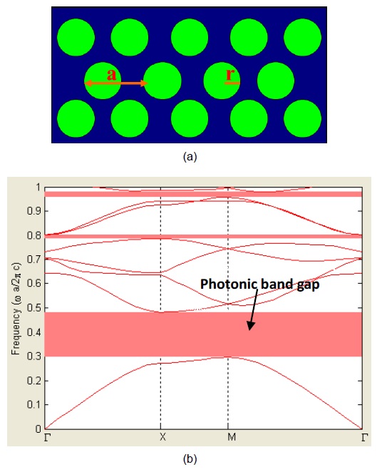
As the light wave propagates inside the photonic crystal, due to the periodic arrangement of the dielectric materials (periodic potential), the light wave experiences multiple scatterings and interferences from various periodic layers. Due to the constructive and destructive interferences in the light traveling path, the amplitude of the propagating light can be increased or decreased depending upon the wavelength and propagation direction of the light. According to the Bloch wave theory, only light modes with a certain eigenfrequency are allowed in the photonic crystal with a certain wave vector. By plotting all of the allowed eigenmodes in the format of eigenfrequency versus wave vector, we can create a photonic band diagram. A photonic band gap can be formed when none of the allowed eigenmodes exist in a certain frequency range. This photonic band gap can be used to appropriately design a photonic insulator in a certain wavelength range.
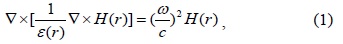
Theoretically, on the basis of Maxwell’s equation, we can describe the photon behavior in a periodically arranged photonic crystal device with a time-varying magnetic field as follows [3]:
where
The plane-wave expansion method (PWEM) solves eigenvalue problems for electromagnetic waves with a periodical potential. PWEM is aneffective method for generating photonic band dispersion diagrams and equifrequency contours for periodic structures. The method expands the unit cell of the periodic dielectric constant function
where

where
In photonic crystal design, refractive index is a critical factor since the origin of the photonic crystal is a periodically varying refractive index/dielectric constant. Therefore, obtaining the accurate refractive index value is of utmost importance. Typically for the sake of simplicity and fast calculation, the effective index method is applied to simplify the three-dimensional (3D) modeling of twodimensional (2D) slab photonic crystals into 2D modeling. In other words, the 3D modeling problems of finite-height slab photonic crystals can be converted into 2D photonic crystal problems with infinite thickness. The greatest advantage of this modification is the dramatic reduction of the number of involved elements and the calculation time.
The effective refractive index (
where
III. VISIBLE WAVELENGTH PHOTONIC INSULATOR DESIGN
The photonic crystal device was designed to have periodically arranged air-hole structures inside a 2D silicon slab with the thickness of 1 μm and arranged in a triangular lattice. It was designed to be similar to a silicon-on-insulator in that the silicon slab sat on top of a thick SiO2 layer. The effective refractive indices used for silicon, air, and glass in this design were 3.46, 1.0, and 1.5, respectively. To design the device effectively, we blocked the visible light wavelengths in the range of 400 to 700 nm and used both theoretical calculations and commercially available software PBGLab (EM Photonics, Newark, DE, USA) to calculate the photonic band diagrams and equifrequency surfaces. MATLAB (The MathWorks Inc., Natick, MA, USA) was used as the computation engine for the software.
Several normalized radii (
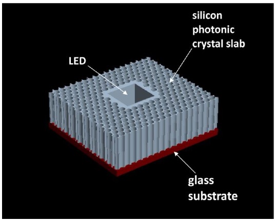
Fig. 2 shows a 3D view of the silicon-based photonic crystal light insulator structure. The silicon slab with airhole arrays sits on top of the glass substrate. The LED is placed in the center of the square trench in the 2D silicon photonic crystal slab and the light emitted from the LED needs to be guided to emit in the perpendicular direction as the silicon photonic crystal structure functions as a light insulator in the horizontal direction.
IV. LIGHT PROPAGATION SIMULATION
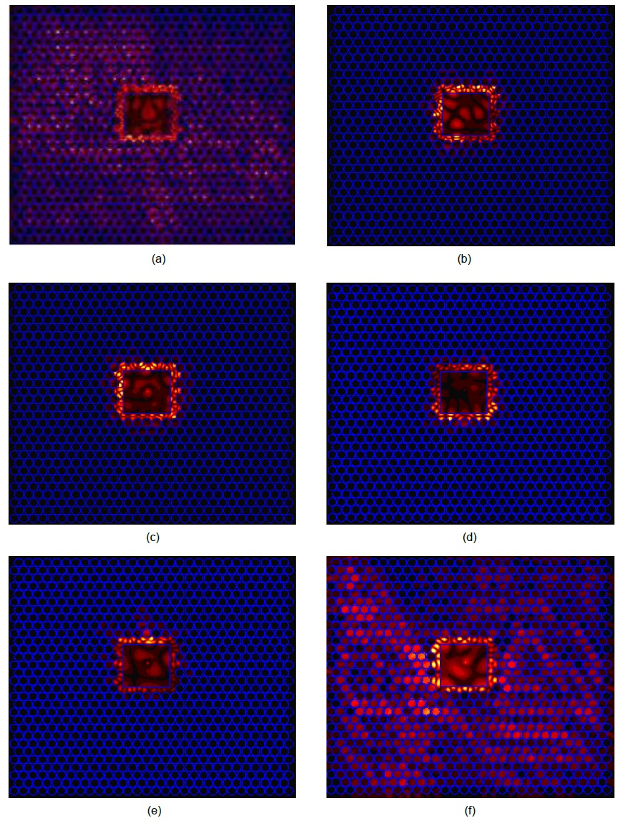
Based on the design parameter achieved by using the PWEM, the 2D and 3D finite-difference time-domain (FDTD) methods were used to find the light propagation characteristics of the device. The simulations were carried out using commercially available software EMPLab (EM Photonics). In the 2D FDTD simulation, a light source with the wavelength of 400, 450, 500, 550, 600, or 650 nm was placed at the center of the square trench where the LED would be placed.
Fig. 3(a) shows the top view of the light propagation characteristic of the device with 400-nm-wavelength light, which clearly shows that some portion of the light leaks in the horizontal direction. However, as the wavelength increases (450–600 nm), as shown in Figs. 3(b)–(e), light propagation in the horizontal direction at these wavelengths was nearly completely blocked and there was no sign of light leakage in the photonic crystal structure. This result clearly shows that the designed photonic crystal device functions as a light insulator for most of the visible light wavelengths in the range of 450–600 nm in the horizontal direction. When the wavelength was increased to 650 nm (Fig. 3(f)), light leakage resumed.
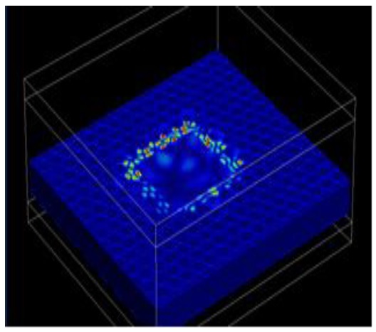
To verify the 2D FDTD simulation results, a 3D FDTD simulation was also carried out. Fig. 4 shows the 3D FDTD simulation result with the point light source wavelength of 500 nm. The result clearly shows the strict confinement of the light only in the square trench in the middle of the device, confirming that there was no light leakage in the horizontal direction. This result agrees well with the 2D FDTD simulation result for 500 nm (Fig. 3(c)).
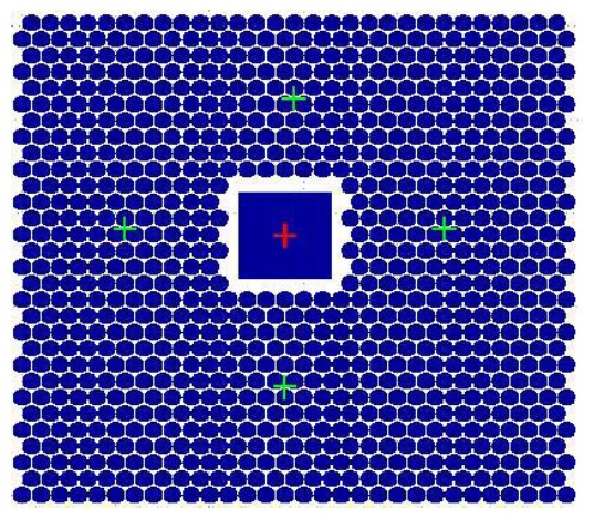
In order to quantitatively understand the light leakage characteristics in the horizontal direction, subsequent simulations were carried out with four detectors placed in the four primary directions of light propagation, as shown in Fig. 5. Again, the light source was placed at the center of the square trench of the device.
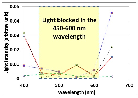
Light intensities at the four light detectors were recorded as the wavelength of the light source changed from 400 to 650 nm. Fig. 6 shows the light intensities as a function of the wavelengths. The four different colors represent the light intensity detection results obtained using four different detectors. It was found that the light intensities at all four detectors are very low in the wavelength range of 440 to 590 nm. This ensures that the designed photonic crystal device works properly to block light propagation in the horizontal direction for most of the visible light wavelengths.
A 2D silicon-based photonic crystal device was designed and simulated as a visible wavelength optical insulator package for an LED light enhancement application. Theoretical modeling as well as PWEM computer modeling was carried out to design the photonic crystal to have a broad range of light insulating properties for visible light wavelengths. Both 2D and 3D FDTD computer simulations were carried out to verify the light blocking properties of the designed silicon-based device. Effective light insulation in the horizontal direction all around the device was demonstrated. The simple assembly of an LED die (irrespective of the material used) into an appropriately designed 2D slab silicon photonic crystal will be beneficial for the enhancement of the light emissionefficiency of LEDs. Such a mix-and-match concept will streamline the manufacturing process of LEDs and can be utilized for the fabrication of photonic crystal-based light insulators required for obtaining high light extraction efficiency.