As projected capacitive touch screen technologies become mature, most smartphones and tablet personal computers (PCs) today employ capacitive touch screens [1, 2]. Recently, these touch screen technologies have been applied to large screens. However, large touch screens are facing serious detection performance issues: they are highly susceptible to ambient noise. Further, as the panel size increases, the sheet resistance and the self-capacitance of indium tin oxide (ITO) films or metal meshes tend to increase. This makes the detection signals (mutual capacitance difference value) suffer from severe attenuation as the signals pass through long paths across the touch screen panel.
While most of the existing touch screen detection schemes use pulse waves for excitation signals, they have a limited scan rate since they apply the excitation pulses sequentially. Recently, a new scheme called frequency division concurrent sensing (FDCS) has been proposed, which applies concurrent sine waves of different frequencies. This scheme can significantly improve the scan rate and the signal-to-noise ratio (SNR) [3-6].
We introduce an efficient differential sensing circuit called a rotating auto-zeroing amplifier (RAZA). This circuit can efficiently cancel the offset of sensing amplifiers without interrupting the output signals, which is a key advantage compared to conventional auto-zeroing amplifiers (AZAs). Therefore, the proposed scheme is particularly effective for continuous analog signals, which are a key component of the FDCS method. In Section II, we briefly describe the architecture of FDCS. In Section III, we present the proposed sensing circuit called RAZA for offset cancellation. Section IV presents the simulation results and compares the SNR measurements with those obtained using the existing schemes. Finally, Section V presents the conclusion.
II. FREQUENCY DIVISION CONCURRENT SENSING METHOD
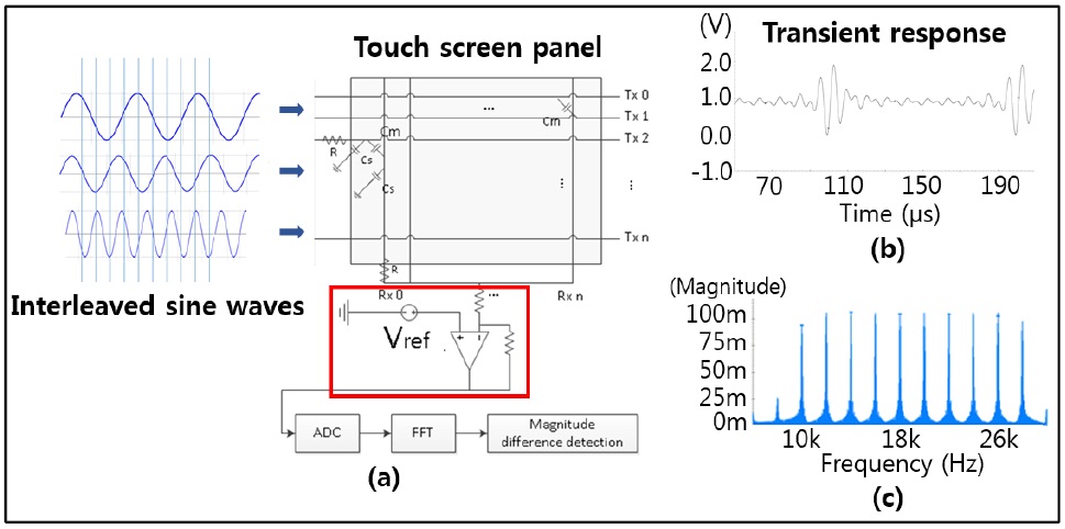
Fig. 1 shows the architecture of an FDCS touch screen controller. Most conventional touch screen detection methods apply excitation pulses and analyze the sensing signals sequentially. Therefore, they are often unacceptably slow for large touch screens. On the other hand, the FDCS technique simultaneously applies sinusoidal signals of different frequencies to all TX lines and analyzes the signals from each sense line in the frequency domain [5].
The sine-wave generator of FDCS applies interleaved sinusoidal signals to each TX line. Each sine wave of a different frequency is applied to each TX line. When TX line increases or decreases, the charge amount in the mutual capacitance of TSP changes. The sensing circuit of FDCS in Fig. 1(a) reads out the sum of all sine waves from each RX line. Fig. 1(b) shows such sine waves read out by the sensing circuit. Then, FDCS converts the sum of the sine waves into the frequency domain by using a fast Fourier transform (FFT) and analyzes the spectral power density. Fig. 1(c) shows such spectral power density. If TSP is touched, the mutual capacitance of the touched cell decreases. The power spectral density of the corresponding frequency also decreases. Then, the touch position algorithm determines the exact locations of the touches. As the sine waves pass through the resistance of the TSP, the signals are significantly attenuated. Therefore, the sensing circuit of FDCS amplifies the attenuated sine waves.
To provide a maximal SNR, the sensing circuit must recover the sine waves without incurring noise and distortion due to the mismatch in its differential amplifier. In this paper, we propose an efficient circuit scheme to cancel the process mismatch or offset of the amplifier.
>
B. Operation of Differential Sensing Circuit
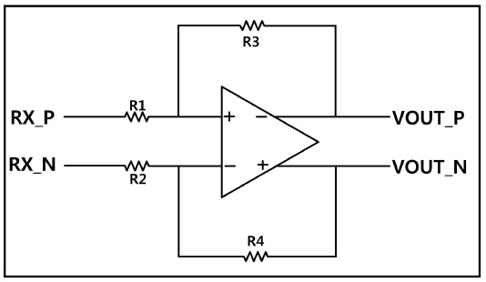
Fig. 2 illustrates a differential sensing circuit that can be used in FDCS. This circuit produces differential outputs VOUT_P and VOUT_N. These outputs are then filtered by a low-pass filter (LPF) and sampled by an ADC. If the RX line under test has no touch, the outputs VOUT_P and VOUT_N should be equal to VCM (common-mode voltage level) assuming that there is no offset. On the other hand, if the RX line has a touch or multiple touches, VOUT_P and VOUT_N show a large voltage swing. Fig. 3(a) shows VOUT_P and VOUT_N waveforms for the case of no touch and the case of having touches assuming that the amplifier has no mismatch or offset.
However, semiconductor circuits almost always have an offset, which is caused by process variation, bias mismatch, power supply mismatch, or low-frequency flick noise. Fig. 3(b) shows VOUT_P and VOUT_N in the case where the differential amplifier has an offset due to its NMOS Gm mismatch. Such offset results in a non-zero output swing even for the no-touch case. Therefore, it can significantly degrade the SNR performance of the touch screen sensing system.
>
C. Differential Sensing Circuit with AZA
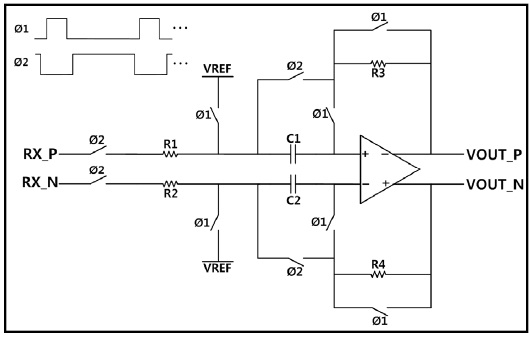
Fig. 4 illustrates a differential sensing circuit for FDCS, which uses a conventional AZA. The differential amplifier in Fig. 4 has a strong advantage over one without an AZA in that it can remove the common-mode noise of the TSP or the power supply noise. However, differential amplifiers often suffer from a mismatch or an offset of the input and the output bias level and the device mismatch of the amplifier’s differential pair due to process variation.
The basic operation of auto-zeroing is the sampling of the unwanted noise and the offset value, and its subtraction from the contaminated signal at the input or the output of an amplifier. The basic auto-zeroing circuit can be used for removing the offset and the low-frequency noise. The correlated double sampling (CDS) technique is an extension of the auto-zeroing method with the sample and hold steps [7-11].
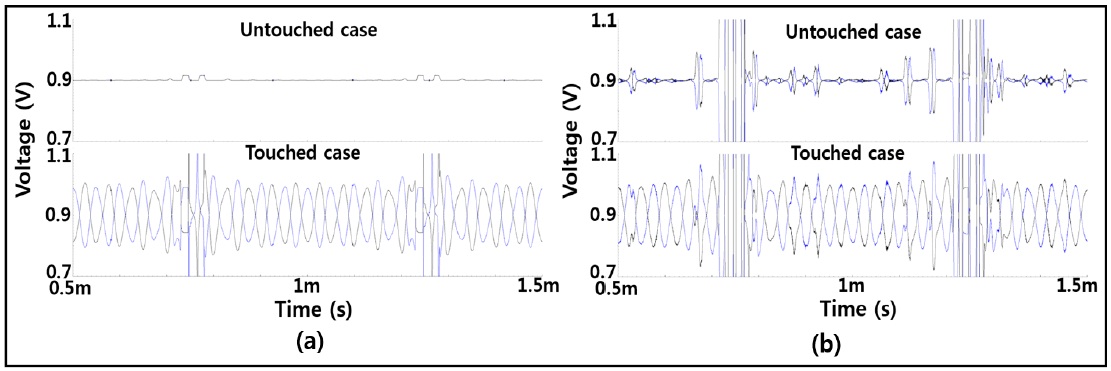
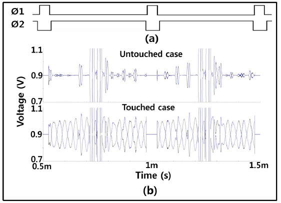
Figs. 5 and 6 show the simulation results of a differential sensing circuit for FDCS using the conventional autozeroing technique. They compare the sensing results for the no-touch and the with touch cases in both the time domain and the frequency domain. In the no-touch case, the amplitudes of the RX_P and RX_N signals are almost the same. Thus, VOUT_P and VOUT_N are nearly flat around the common-mode voltage.
The auto-zeroing circuit shown in Fig. 4 cancels the offset as follows: it captures the offset value of the OP Amp during ø1 and amplifies the input signal during ø2. During ø1, C1 and C2 store the voltage difference between VREF and the positive input of the OP Amp. During ø2, the OP Amp operates in the normal mode and amplifies the voltage difference between RX_P and RX_N along with the captured offset voltage.
However, the drawback of this auto-zeroing circuit is that the amplifier stops normal operation and thus, loses the signal during ø1. Therefore, it cannot work properly with continuous analog signals. This causes a serious problem for FDCS touch screen sensing schemes, which use continuous analog sine waves. FDCS needs an analog anti-aliasing filter before ADC (as shown in Fig. 7), and therefore, a fast switching circuit such as a switched capacitor amplifier with CDS is not a suitable solution.
Touch screen panels receive various types of noise, such as noise from the power supply, LCD, and the surrounding environment. Such noise tends to be more prominent in large touch screens. A considerable amount of noise can corrupt the small RX signals from TSPs and make it difficult for touch detection techniques to achieve a high SNR.
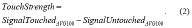
Eqs. (1)–(3) present the SNR calculation. This SNR calculation method is commonly used in the touch screen sensor industry. It accurately estimates the strength of the sensed signals and the noise power from a large number of RX signal samples, including the ambient and LCD noise. By using these equations, we measure the SNR performance of various sensing circuits and compare them in Section IV [12, 13].


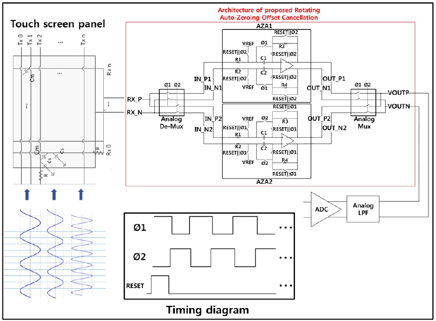
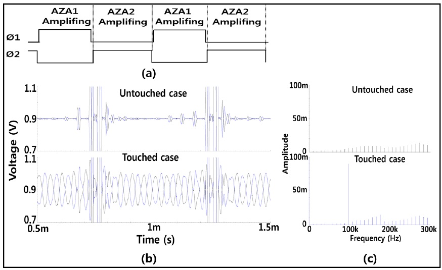
Rotating Auto-Zeroing Offset Cancellation: To improve the drawback of the conventional auto-zeroing described in Section II-C, we propose a rotating auto-zeroing offset cancellation scheme. As illustrated in Fig. 7, it consists of an analog mux, an analog de-mux, and two AZAs.
The proposed scheme alternates the two AZAs to avoid losing the signal during the offset capturing process. It uses one AZA to capture its offset while using the other AZA to amplify the signal. In Fig. 7, ø1 and ø2 are non-overlapping opposite control signals that select the operation modes. When ø1 is high, AZA1 is in the amplify mode and AZA2 is in the offset capture mode. In contrast, when ø2 is high, AZA1 is in the offset capture mode, while AZA2 is in the amplify mode.
The analog de-mux in Fig. 7 feeds the input signals to either AZA1 or AZA2. When ø1 is high and ø2 is low, RX lines are connected to AZA1’s IN_P and IN_N, and thus, AZA1 conducts its amplification. During this time, AZA2 captures its offset. On the other hand, when ø1 is low and ø2 is high, RX lines are connected to AZA2, allowing AZA2 to conduct its amplification. The analog mux in Fig. 7 forwards AZA1’s or AZA2’s outputs to the analog LPF. The analog LPF removes the aliasing of high-frequency noise before the ADC process. Therefore, the proposed scheme can effectively cancel the offset without incurring signal interruption and switching noise and is well suited for touch screen sensing methods using continuous analog signals.
We designed a sensing circuit for an FDCS SoC by using the proposed rotating auto-zeroing offset cancellation scheme. We implemented the SoC by using a Magnachip/ SK Hynix 0.18-µm CMOS process.
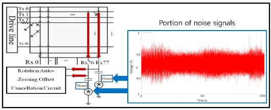
For the realistic simulation results, we used Cadence SPECTRE with an accurate TSP model and noise source. To measure the realistic performance of the proposed circuit, we inserted noise signals into each RX line. We also applied an asymmetric device size (10% MOS size mismatch) to the OP Amp design in order to measure the effectiveness of offset cancellation. Fig. 8 illustrates the TSP model and the noise source used for the realistic simulation results. It shows a portion of the noise signal, which is the realistic noise data provided by Kortek and a leading touch screen panel manufacturer. Fig. 9 shows the simulation results of the proposed RAZA.
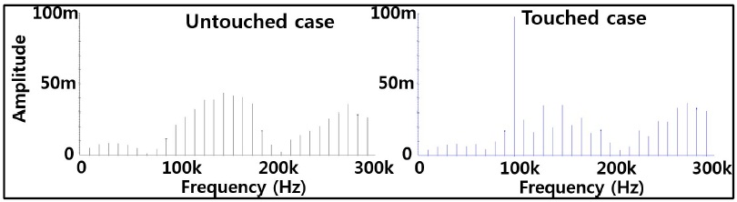
Fig. 9(b) shows the results in the time domain. The upper waveform is the case of no touch, and the lower waveform is the case of a touch using nine sine waves of 100–190 kHz for nine TX lines. In the case of no touch, the time-domain output signals are nearly flat around the common-mode voltage. Small differential signals still exist because the sine waves pass through different paths of TSP and experience different parasitic resistance and capacitance. At the end of each frame period, the time-domain result shows a large output amplitude. This is because the accumulation of the output sine waves creates a periodic peak value with the sum of each sine wave’s amplitude. In the case of touch, the mutual capacitance of the touched cell decreases. This change makes the sine wave corresponding to the touched TX line appear as a relatively large differential RX signal. In contrast, other sine waves appear as nearly zero differential RX signals.
In the frequency domain, the sine wave passing through the touched cell appears as a peak spectral density, while other sine waves show a very small spectral density. By finding the peak values of the spectral density for each RX differential pair, the FDCS scheme determines which TX lines and RX lines have been touched.
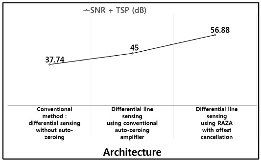
Fig. 10 compares the SNR measurement of three differential sensing schemes: without auto-zeroing, with conventional auto-zeroing, and with the proposed scheme. The proposed scheme using RAZA provides an SNR gain of 56.88 dB (46.84 – (–10.04) dB), which was measured using the TSP model and the noise source described above.
It presents an SNR improvement of 19 dB compared to the result without auto-zeroing, and an improvement of 12 dB compared to the conventional auto-zeroing scheme. This is a substantial improvement that is required for the FDCS touch screen detection method to provide a high performance for large touch screens. The conventional autozeroing scheme shows a relatively low SNR because it loses the sensing signal in the offset capture period.
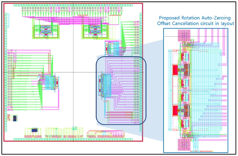
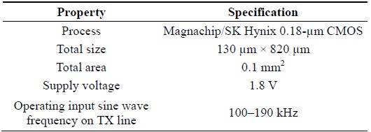
Fig. 11 shows the layout result of the proposed sensing circuit, which was described in Fig. 7. Table 1 summarizes the design result of the proposed sensing circuit. We implemented the chip using a Magnachip/SK Hynix 0.18-µm CMOS process. The size of the circuit that we implemented was only 0.1 mm2, which is sufficiently small for most touch screen controller SoCs. For FDCS driving signals, we applied nine sine wave signals to the TX lines with frequencies from 100 to 190 kHz.
[Table 1.] Specifications of proposed auto-zeroing offset cancellation

Specifications of proposed auto-zeroing offset cancellation
In this paper, we have proposed an efficient offset cancellation scheme that is well suited to differential sensing circuits with continuous analog excitation signals. The proposed scheme using RAZA can cancel the offset of sensing circuits without losing the signal during the offset capture cycle. This allows a touch screen sensing method such as FDCS to drive and sense continuous analog sine waves, which was not possible with the conventional auto-zeroing schemes. Experimental results show that the proposed scheme provides an SNR improvement of 12 dB compared with the conventional auto-zeroing scheme. Therefore, the proposed scheme can be considered a key component of high-performance touch screen detection methods with continuous analog signals.

![Proposed frequency division concurrent sensing (FDCS) scheme: (a) FDCS architecture, (b) transient response of the RX output, and (c) frequency response of the RX output [6].](http://oak.go.kr/repository/journal/17344/E1ICAW_2015_v13n3_189_f001.jpg)