Touch screen panels (TSP) have been widely used in electronic devices such as TVs, mobile phones, and laptops. [1] The application area has been broadened with the increasing demand for intuitive user interfaces. [2-4] A resistive TSP senses the resistance change caused by the deformation of the TSP film. [5] It is possible to make a low-cost and high-resolution TSP with the resistive sensing mechanism. However, there are some difficulties in achieving multi-touch functionality, durability, and transparency. On the other hand, a capacitive TSP senses the capacitance change driven by finger capacitance. [6] The capacitive TSP is more costly in fabrication and more problematic to be made in large scale than the resistive counterpart. However, the capacitive TSP has its strength in high resolution and multi-touch functionality. With its multi-touch availability and also durability, the capacitive TSP is preferable in tablet PC and mobile phone applications. [7] A transparent electrode is another important component of a TSP. Several materials including indium tin oxide (ITO), graphene, carbon nanotube (CNT), and metal nanowires have been evaluated for fabricating transparent electrodes of a TSP. [8-12] Although ITO has been used most extensively for TSP electrodes thanks to its high transmittance and low resistance, its brittleness is a severe obstacle to being used as flexible TSP electrodes. Silver nanowire (AgNW) is considered to be one potential replacement for ITO for flexible TSP electrodes. In addition to flexibility, there are some other benefits obtainable by replacing ITO with AgNW such as material cost reduction, panel thickness reduction, higher transmittance, and higher touch sensitivity. Recently, the haze effect which is one weak point of AgNW has also been improved. [13] Thus, AgNW seems to be a quite promising candidate material for making flexible and transparent electrodes of TSP. There have actually been several experimental works reporting the fabrication of flexible and transparent TSP based on AgNW electrodes. [14-16] In this study, we fabricated a highly flexible and transparent capacitive TSP by using AgNW crossing electrodes and Al-doped ZnO (AZO) bridge electrodes formed on top of SU-8 bridge insulators. The continuity of the thin bridge electrode was improved significantly by reducing the side-wall slope of the bridge insulator with scattered-light exposure in the photolithography process. This scattered-light exposure can be an easily-applicable experimental method to ensure the reliability of any flexible TSP adopting bridge structures.
Among all the fabrication processes in our work, the most relevant process is the one for making flexible and transparent bridge insulators with low side-wall slope. In this section, we describe the entire process for fabricating a flexible and transparent TSP sample with a focus on the step to make bridge structures.
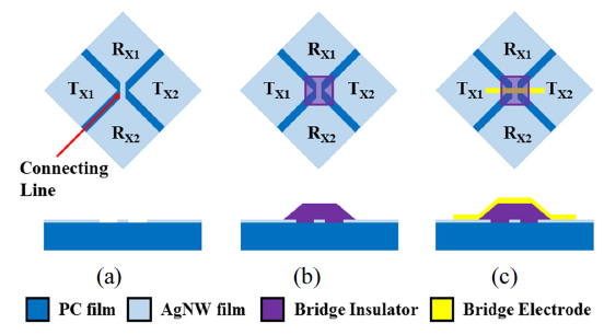
The fabrication flow consists of three major steps, which are the patterning of AgNW electrodes, the formation of bridge insulators, and the formation of bridge electrodes. Figure 1 shows the entire fabrication flow together with the plane and cross-sectional schematic views of the patterned structure in each individual step. In the first step, an AgNW film coated on a polycarbonate (PC) film was patterned by using the conventional photolithography process to form driving electrodes (Tx) and sensing electrodes (Rx). The positive AZ5214E photoresist was used and the AgNW film on the developed area was etched with a commercial Aluminum etchant (Al ETCH TYPE A, TRANSENE Inc.). After etching, the remaining photoresist was removed with acetone. As shown in Fig. 1(a), both Tx and Rx electrodes contain diamond-shape patterns but only Rx electrode diamonds are connected to their nearest neighbors by the connecting line in the first step. The touch sensing is accomplished by analyzing the capacitance change sensed by the Rx electrode while a finite voltage is applied on the Tx electrode. Here, R stands for “Receiver” and T “Transmitter”.
In the second step, the bridge insulator covering the connecting line of Rx electrodes were formed in order to prevent the electrical connection between the Tx and Rx electrodes (Fig. 1 (b)). The bridge insulator acts also as a capacitor for touch sensing. If using the conventional photolithography process, the side-wall of the bridge insulator is formed to be quite vertical, which makes it quite difficult to have the robust connectivity of the bridge electrode. It is necessary to keep the bridge electrode thin enough for high transparency of the TSP. Hence, the coverage of the bridge electrode over the bridge insulator with vertical sidewalls can be bad even when the electrode film is deposited with a conformal deposition method such as atomic layer deposition (ALD). This unstable film connection causes high resistance of the Tx electrode. One efficient way to secure the connectivity of the bridge electrode is to form the bridge insulator with low side-wall slope. It was found that the low side-wall slope of bridge insulator could be achieved by utilizing the UV light scattered from the substrate during the exposure step of the photolithography process. We chose SU-8 as the bridge insulator material. SU-8 is a transparent negative photoresist which has been considered to be suitable for bridge insulators. [17, 18]
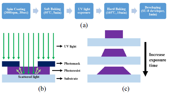
As shown in Fig. 2(a), the SU-8 layer was first spin-coated over the patterned Tx and Rx electrodes at 3000 rpm for 30 sec and its thickness reached ~500 nm. After soft-baking at 95 ℃ for 5 min, the coated SU-8 layer was exposed to UV light through a photomask and it was then hard-baked at 105 ℃ for 10 min. Lastly, the whole sample was dipped into SU-8 developer for 1 min so that the SU-8 layer unexposed to UV light was removed (negative photoresist). Fig. 2(b) shows how the UV light scattered from the substrate can affect the shape of the bridge insulator side-wall. The scattered light is weaker than the direct light collimated from the UV source. Thus, the scattered light is almost ignorable when the exposure time is optimally adjusted to entangle SU-8 polymers uncovered by the photomask. This exposure condition is normally preferred to get a sharp pattern identical to the photomask pattern by minimizing the effect of scattered light. In our work, however, the exposure time was extended intentionally to enhance the effect of scattered light. With the overdose of UV light, some part of SU-8 layer near the uncovered region can get enough scattered light to entangle SU-8 polymers. Since the scattered light propagates spherically outward from the scattering points on the substrate, the exposure to scattered light will be significant only in the lower part of the SU-8 layer around the uncovered region (Fig. 2(b)). Hence, the cross-sectional shape of bridge insulator after the developing step will be more like a trapezoid rather than a rectangle as shown in Fig. 2(c). As the amount of overdose increases, the side-wall slope of bridge insulator becomes lower due to the lateral extension of the region exposed to the scattered light by the amount for entangling SU-8 polymers (Fig. 2(c)). The exposure time for overdose was determined to be 10 times the optimized exposure time for forming vertical side-walls. The optimized exposure time is estimated from the following relation.
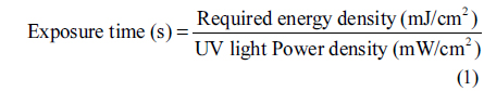
Here, the required energy density is 100 mJ/cm2 for SU-8 photoresist.
After the bridge insulator with low side-wall slope was formed, an AZO thin film was deposited on the sample surface by using ALD (LUCIDA D100 system, NCD Corporation, South Korea). The ALD deposition temperature of AZO film was set at 150 ℃ to protect the patterned AgNW electrode. It is known that the AgNW film should NOT be heated over 200 ℃ for its stability. The AZO film was deposited under constant N2 flow (50 sccm) by using Di-Ethyl-Zinc (DEZ), Tri-Methyl Aluminum (TMA), and water (H2O) as precursors. One complete ALD cycle was composed of 0.2 sec pulse of DEZ and H2O followed by 10 sec pause and 0.2 sec pulse of TMA and H2O followed by 10 sec pause. Once all ALD cycles were completed, N2 flow increased to 500 sccm and continued for 3 min as a post process. Two different Al doping concentrations (2%, 5%) were tested to find the optimal conductivity and visible light transmittance. The 2% doping was achieved with the ALD sequence of 49 DEZ cycles per one TMA cycle and the 5% doping with 19 DEZ cycles per one TMA cycle. Based on the working principle of ALD, the deposited AZO film is conformal and this is also beneficial for the good connectivity of bridge electrode. Finally, the bridge electrode was formed by patterning the deposited AZO film with the conventional photolithography and wet etching. For the wet etching process, the FeCl3 etchant was used since it could etch the AZO film selectively without damaging the AgNW electrode.
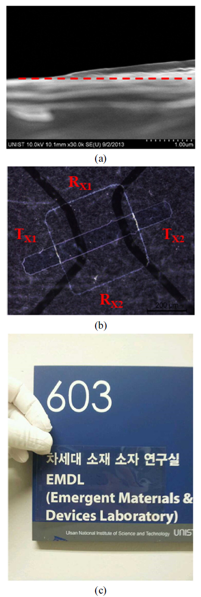
Figure 3(a) is the cross-sectional scanning electron microscope (SEM) image of the bridge insulator formed with low side-wall slope. The dotted red line is the boundary of the bridge insulator and the AgNW electrode. The thickness of the bridge insulator is around 500 nm in the flat area and it decreases gradually from the position where the side-wall slope begins down to the edge. The edge of bridge insulator does NOT have any abrupt jump in height, ensuring the continuous coverage of the bridge electrode deposited over it. Fig. 3(b) is the optical microscope image of a completed TSP sample. The image was captured in dark-field mode in order to make the transparent device structure visible. As designed in Fig. 1(c), the Rx electrode diamonds are connected with a thick connecting line. The Tx electrode diamonds are connected with the rectangular bridge electrode formed over the square bridge insulator. The resistance between the Tx electrode diamonds was measured to be 6.5 kΩ while the resistance between the Rx electrode diamonds was measured to be ~1 kΩ. The somewhat larger resistance between the Tx electrode diamonds is considered to be mainly due to the larger sheet resistance of AZO film than the AgNW film. Fig. 3(c) demonstrates how transparent the fabricated TSP sample containing an array of crossed Rx and Tx electrodes is.
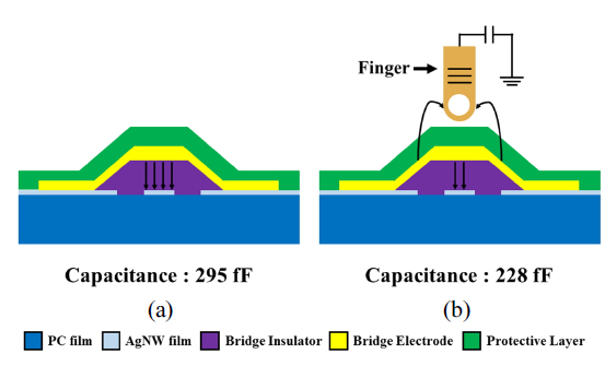
Figure 4 shows the operational principle of the fabricated TSP sample. Before touching the panel with a finger (Fig. 4(a)), the capacitance of the bridge insulator is measured while applying a voltage on the driving Tx electrode. The electric field lines (black lines) are heading mostly to the Rx electrode connecting line. When the panel is touched by a finger, the finger can act as another electrode and some electric field lines will go into the finger (Fig. 4(b)). [20] In this case, the amount of charges held by the bridge insulator becomes smaller and the capacitance of the bridge insulator is measured to decrease. The charges lost from the bridge insulator will be held by the protective layer covering the TSP. The measured capacitance of the fabricated TSP was 295 fF before touching and it decreased to 228 fF during touching. The rate of change was 22.71% which is quite enough to recognize the signal difference. The capacitance can be roughly calculated by the following equation assuming the parallel plate capacitor.

The capacitor area (
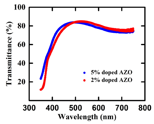
Since the area of the AZO bridge electrode on the fabricated TSP is too small to measure the optical transmittance through the electrode, we fabricated separate samples for measuring the transmittance of AZO film. Two 1cm by 1cm PC films each of which had an AgNW film coated on the surface were prepared. AZO films with two different Al-doping concentrations (2%, 5%) were deposited by using the same ALD processes for the TSP sample fabrication. Figure 5 shows the measured transmittances of the AZO/AgNW/PC stacks in the visible light range by using a UV-vis NIR spectrometer (Agilent). The transmittance difference for different Al-doping concentrations is not significantly large in the visible light range. In actuality, the 2% doped AZO film has slightly larger transmittance in the visible light range, which is to be expected for lower doping concentration. However, both films are adequate for the bridge electrode of highly transparent TSP. The sheet resistance of 2% doped AZO film was measured to be ~140 Ohm/sq and that of 5% doped AZO film be ~130 Ohm/sq. It seems that the actual Al doping of ZnO during ALD deposition is not quite tunable due to the solubility limit of Al in ZnO. The electrical properties of both films are also good enough to be used as the bridge electrode material.
In summary, we have fabricated a highly flexible capacitive TSP by using AgNW electrodes and transparent bridge structures. The bridge structure is composed of an SU-8 bridge insulator and an AZO bridge electrode. In order to form the bridge electrode connecting the AgNW electrode diamonds in stable and robust manners, we made the side-wall slope of the bridge insulator as low as possible by extending the exposure time of the photolithography process beyond the optimized value for forming vertical side-walls. With the extended exposure time, the lower part of the SU-8 layer around the region uncovered by the photomask can be exposed enough to the UV light scattered from the substrate, leading to the formation of a bridge insulator with low side-wall slope. We have also developed the ALD process to deposit the AZO film for patterning the bridge electrode at relatively low temperature, 150 ℃. The deposited AZO film was measured to have low sheet resistance and high optical transmittance in the visible light range. The fabricated TSP sample showed good touch-sensing performances. The capacitance change between