Pulse-width modulation (PWM) is a well-known technique in the electrical domain and is used in several applications, such as telecommunications, power delivery and speed control, voltage regulation, inverters, and audio effects and amplification. In telecommunications, widths of pulses are used to specify data values, which are encoded at one end and decoded at the other [1]. PWM can be used to control the amount of power delivered to a load without incurring the losses that would result from linear power delivery by resistive means [2]. In efficient voltage regulators, PWM is used to switch voltage to the load with an appropriate DC to approximate an output voltage at the desired level [3, 4]. PWM is also used in sound (music) synthesis, in particular subtractive synthesis, as it gives a sound effect similar to a chorus, or slightly detuned oscillators played together [5]. Since electrical PWM is not suitable for applications where an electrically isolated amplifier is required (
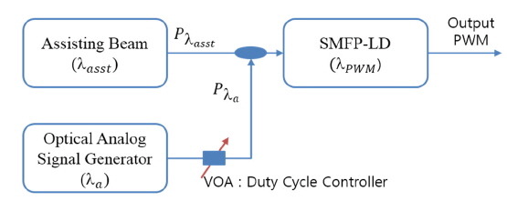
A simple electrical PWM generator is composed of three functional parts [13]: an analog input, a reference, and a comparator. The comparator provides high output (ON) when the input value is less than the reference, and low output (OFF) when the input value is greater than or equal to the reference. Hence, based on the inequality between the analog input (typically a saw-tooth, ramp, triangle, or sinusoidal wave) and the reference, the comparator will provide a square wave as output (digital output) with tunable ON/OFF duration. Figure 1 shows the block diagram of the proposed OPWMG, where the output PWM signal is taken after the optical bandpass filter (OBF) at wavelength λPWM. The SMFP-LD used in our experiment was specially designed and developed in our laboratory to have a dominant self-locked mode with a high side-mode-suppression ratio [13]. To shorten the SMFP-LD’s recovery time after being injection-locked by the analog signal from an optical analog signal generator, the assisting light beam’s wavelength λasst is set to be the same as that of the SMFP-LD’s dominant self-locked mode (λasst=λPWM). In this proposed scheme, the assisting beam power Pλasst is kept constant; the assisting beam is used to help the SMFP-LD’s self-locked mode to recover the unlocked state quickly, which can yield better output waveforms. The SMFP-LD in the proposed scheme has the property of bistability [14], which is explained as follow: When the SMFP-LD is injected with appropriate power from an external light beam at a wavelength close enough to one of the SMFP-LD’s side modes, it is fully injection-locked, and all of its side modes are suppressed. That power level is called
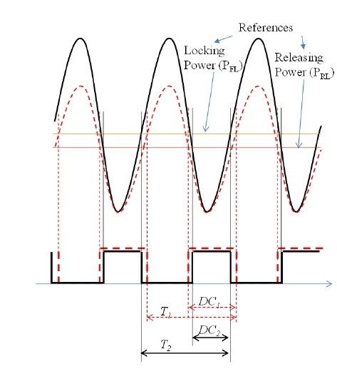
According to the injection-locking and bistability properties of the SMFP-LD, the locking duration can be varied when the power differences (Pλa - PFL and Pλa - PRL) are varied. In other words, the DC can be varied as the change of Pλa compared to PRL and PFL. In this proposed scheme, Pλa is varied to control the relative difference between Pλa and PFL/PRL. It is noted that when λa, λasst, and Pλasst are constant, only power from the analog input contributes to the control of PWM’s DC. In fact, PRL and PFL can be changed, depending on the wavelength detuning of λa to the corresponding side mode of the SMFP-LD; however, in this paper we only focus on one specific wavelength detuning.
Figure 2 shows the relationship between Pλa and the output power, where the red dashed and black solid lines represent respectively the states of the analog input and output PWM signals before and after increasing Pλa. Pλa is controlled by the VOA after the MOD, as shown in Fig. 3. When Pλa is increased, more of the sinusoidal wave is above the locking power, and the locking duration is increased, or, in other words, the DC is decreased (DC2 < DC1). It is noted that the period is unchanged, if the analog input period (T) is constant (T2 = T1 = T). In conclusion, optical PWM signals can be generated in the optical domain, and the PWM’s DC can be controlled by varying the power of the analog input.
III. EXPERIMENTAL SETUP AND RESULTS
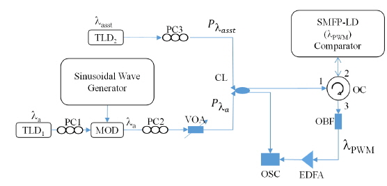
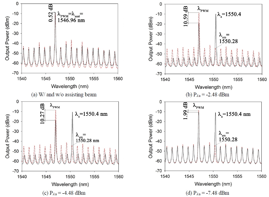
Figure 3 shows the experimental setup of the OPWMG where the threshold current, bias current, and temperature of the SMFP-LD are 11 mA, 19 mA, and 25.3℃ respectively. Under these working conditions the SMFP-LD has dominant modes at λPWM = 1546.96 nm. The optical analog input has a wavelength of 1550.4 nm, corresponding to the SMFP-LD’s side mode wavelength of 1550.28 nm (wavelength detuning Δλ = 1550.4 − 1550.28 = 0.12 nm). The assisting beam’s wavelength λasst was set to be the same as that of the SMFP-LD’s self-locked mode (λasst = λPWM = 1546.96 nm), and its lasing power was fixed at about −10.70 dBm (measured before the optical circulator). When the assisting beam was turned on, the SMFP-LD was fully locked for Pλa ≥ −5.77 dBm, and the SMFP-LD’s full-lock state was released for Pλa ≤ −6.68 dBm. Actually, the locking state was not fully released even when the input power was less than −6.68 dBm; we still observed the weak-lock phenomenon, where the self-locked mode power was reduced but not fully eliminated. The polarization controller PC1 is used to minimize the polarization-dependent loss in the Mach-Zehnder modulator (MOD), and PC2 and PC3 are used to maximize the TE optical powers that are injected into the SMFP-LD. Due to the injection-locking property of the FP-LD, the more TE power that is injected into the SMFP-LD, the greater the suppression of its side modes and the higher the power at the injected mode.
Figure 4 presents the spectra at the output of the SMFP-LD before the OBF, where in Fig. 4(a) the red dashed line represents the SMFP-LD spectrum only (assisting beam and analog input are turned off) and the black solid line represents the SMFP-LD spectrum when only the assisting beam is turned on. In this figure we can see the weak-lock phenomenon, where side-mode powers are reduced a little but not fully suppressed. In Figs. 4(b), 4(c), and 4(d) the red dashed line represents the spectra of the SMFP-LD when only the assisting beam is ON, and the black solid line represents the spectra of the SMFP-LD before the OBF when both assisting beam and optical analog input are ON (Pλa = −2.48, −4.48, and −7.48 dBm respectively). We can see the full-lock phenomena in Figs. 4(b) and 4(c), where all side modes of the SMFP-LD are deeply suppressed because Pλa (−2.48 and −4.48 dBm) is above the full-lock power level PFL = −5.77 dBm, whereas the full-lock state is released (all side modes are recovered) in Fig. 4(d) because Pλa = −7.48 dBm, which is below the release power level PRL = −6.68 dBm.
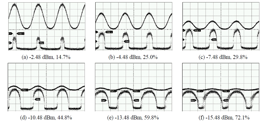
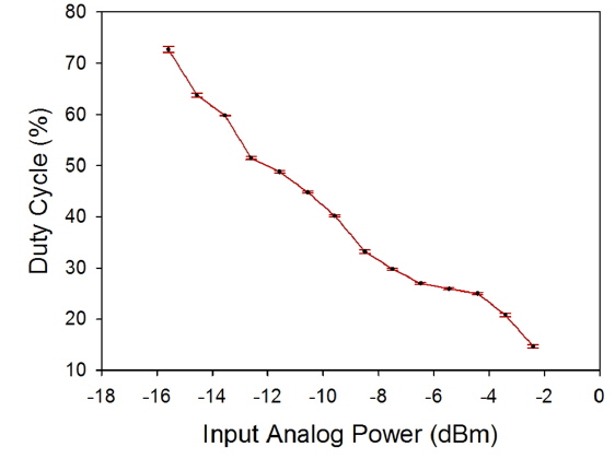
Figure 5 shows optical sinusoidal waveforms of the analog input signal taken before the optical circulator (OC), and the output optical PWM signal taken after the EDFA. The analog optical sinusoidal source is operated at a frequency of 16 MHz, and the oscilloscope has a time resolution of 20 ns/div. In Fig. 5, the input and output waveforms appear to be almost in phase, contradicting their working principle, which is out of phase, as shown in Fig. 2. The reason is that the time difference between the two light paths traveled to the oscilloscope (OSC) is about one period, which is equivalent to 12.5 m of optical fiber. The output PWM has DCs of 14.7%, 25.0%, 29.8%, 48.8%, 59.8%, and 72.1%, corresponding to Pλa = −2.48, −4.48, −7.48, −10.48, −13.48, and −15.48 dBm respectively.
By changing the analog sinusoidal source power in intervals of about 0.5 dB, we measured the DC of the proposed OPWMG, as shown in Fig. 6. In this figure the DC versus Pλa curve has a resolution of about 4.399 %/dB. The measurement process is taken as follows: The value of each data point on the curve (represented by a black dot) was the average of 5 readings of the DC value (20-second interval) from the OSC. The error bars, which are included for every data point on the curve, reflected the standard error based on the recorded DC values. The reading error is seen to increase at low input power, which may arise from the increase in mode-partition noise of the SMFP-LD when the input analog power is low [17], and also from the mode beating between the injected and self-locked modes. The highest observed standard error was about 0.6% at input power of −15.48 dBm. If the input power is above −2.48 dBm, all modes of the single mode FP-LD are collapsed (DC = 0). If the input power is below −15.48 dBm, the locking state is unstable and the output signal so noisy that the output DC cannot be identified. When we decreased the input power about 1 dB more, the locking state was destroyed totally (DC = 100%).
We have proposed and experimentally verified an optical PWM generator, which is based on the injection-locking property of an external cavity-based single-mode FP-LD. The OPWMG can directly generate a PWM signal in the optical domain with a working frequency of 16 MHz, a duty cycle range between 14.7% and 72.1%, clear output waveforms, and duty cycle resolution of about 4.399 (%/dB). The PWM’s duty cycle can be varied by tuning the power of the optical analog input. It is possible to increase the working frequency of the OPWMG up to several GHz, because the proposed scheme is based on injection-locking of an SMFP-LD. Indeed, several works have been based on injection-locking of SMFP-LD showing working frequencies up to 10 GHz, such as those are reported in [15, 16]. An Optical PWM possesses significant advantages for applications that require strong immunity to EMI (