The prospect of optical processing has extensively motivated recent activities for overcoming the essential performance constraints of semiconductor electronic devices, which suffer from inherent delay and high heat generation. Photonic devices, which use photons as information carriers, can provide high speed, high capacity, and low loss components [1].
The development of all-optical logic technology is important for a wide range of applications in all-optical networks, including high-speed all-optical packet routing and optical encryption [2]. An important step in the development of all-optical logic technology, which includes key functionalities at the fundamental and system levels such as buffering, demultiplexing, clock recovery, packet processing, wavelength conversion, data regeneration, and optical encryption/decryption, is the demonstration of optical logic elements that can operate at ultrahigh speeds [3].
All-optical processing has many other applications, such as add-drop multiplexing, simple bit-pattern recognition, address recognition, header processing, switching, and packet synchronization [4, 5]. Addition is one of the most important operations in Boolean functions and is used in arithmetic logic units and to perform packet-header processing [6].
The operation of a half adder/subtractor arithmetic using dark-bright soliton conversion control has been reported by Phongsanam et al. [7]. Many designs for a single adder or adder with subtractor have been proposed using a semiconductor optical amplifier (SOA) and periodically-poled lithium niobate (PPLN) waveguide [8], a microring resonator [9], exploitation of four-wave mixing (FWM) in a SOA [10], a three-state system [11], a terahertz optical asymmetric demultiplexer (TOAD) [12], a single-slot waveguide [13], two SOAs [14], and an SOA assisted by an optical bandpass filter [15]. Most of these implementations involve half addition and/or subtraction operations. Fiber-based logic implementations are bulky and not integrable. Frequency-encoding techniques using PPLN waveguides make these implementations temperature and polarization sensitive. Proposals based on polarization-based logic implementation have some drawbacks, as the state of polarization may change at the reflecting or refracting points along the transmission or propagation path. SOA-based all-optical signal processing has demonstrated great potential in terms of high speed, low power consumption, and optical integration [16].
Only a few works have reported on an all-optical full adder implementation, but with different schemes. Scaffardi et al. have introduced an all-optical full adder by cascading a basic gate that exploits cross-gain modulation and cross-polarization rotation in a SOA [6]. The setup includes eight basic logic gates, five erbium-doped fiber amplifiers (EDFAs), ten fixed delays, and many other circuit elements to implement the adder. EDFAs and other circuit elements may result in large physical size of the full adder, which inhibits integration.
In this communication we propose a new and potentially integrable scheme for realizing an all-optical binary full adder employing two XOR gates, two AND gates, and one OR gate. The XOR gates are realized using a Mach-Zehnder interferometer (MZI) based on a semiconductor optical amplifier (SOA). The AND and OR gates are based on the nonlinear properties of a semiconductor optical amplifier. The proposed adder requires the minimum number of active components, thus reducing complexity and power consumption. Successful operation of the adder is demonstrated at 10 Gb/s using return-to-zero (RZ) modulated signals.
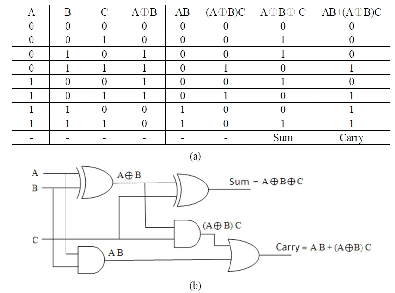
The full adder is a combinational logic circuit, performing the addition of three binary digits. It is usually a component in a cascade of adders, which add 8-, 16- or 32-bit binary numbers. A one-bit full adder adds three one-bit numbers such as A, B, and C in which A and B are the operands, and C is a bit carried in from the previous less-significant stage. Figure 1(a) presents the truth table for an all-optical 2-bit binary full adder, showing that the Carry output is in logic state 1 only when at least two inputs are at logic level high. Otherwise, it is in logic state 0. The Sum bit represents the least significant bit of the three-bit binary summation.
Figure 1(b) depicts a conventional electronic 2-bit adder layout comprised of two XOR gates, two AND gates, and a logical OR gate. The two input data bits A and B are applied to the first XOR gate. The output of this XOR operation is XORed again with a bit carried in from the previous less-significant stage (input bit C) to produce the Sum output. The two input operands A and B are ANDed, then the output of the first XOR gate is ANDed with input bit C. Finally, the outputs of the two AND gates are ORed to produce the Carry output.
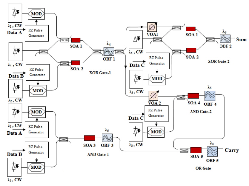
The proposed architecture for the all-optical full adder is shown in Fig. 2. It consists of two XOR gates (XOR Gate 1 and XOR Gate 2), two AND gates (AND Gate 1 and AND Gate 2), and one OR gate. The XOR gates are realized using SOA-based MZIs with the same SOA placed in each of the arms. The wavelengths of five continuous-wave (CW) beams generated by laser diodes are 1553.32 nm (λ1), 1552.52 nm (λ2), 1550.12 nm (λ3), 1550.92 nm (λ4) and 1551.72 nm (λ5) respectively.
Two optical input data signals A and B at wavelengths of 1553.32 nm (λ1) and 1552.52 nm (λ2) respectively, and a CW control signal at wavelength 1550.92 nm (λ4), are applied to XOR Gate 1 of the full adder. A Gaussian tunable optical bandpass filter (OBF1) of 0.4-nm bandwidth is used to filter out the A XOR B signal at a wavelength of 1550.92 nm (λ4). The output of XOR Gate 1 and input carry signal C (1550.12 nm (λ3)) act as input signals to XOR Gate 2. A CW signal at a wavelength of 1551.72 nm (λ5) is applied as a control signal to this XOR gate. OBF2 is used to filter the Sum output at a wavelength of 1551.72 nm (λ5).
AND Gate 1 is used to logically AND the input data signals A and B. The output of XOR Gate 1 at a wavelength of 1550.92 nm (λ4) and the input carry signal C (1550.12 nm (λ3)) are applied to AND Gate 2. AND Gate 1 and AND Gate 2 are implemented by means of the FWM effect in SOA3 and SOA4 respectively. When input data signals at different wavelengths are present in the SOA, the conjugated light is generated due to the FWM effect, which is optically filtered to implement AND logic. Tunable Gaussian narrow optical bandpass filters OBF3 and OBF4 with a bandwidth of 0.32 nm are used to filter the AND logic.
SOA5 and OBF5 constitute a logical OR gate. The outputs of AND Gate 1 and AND Gate 2 at a wavelength of 1551.72 nm (λ5) are applied to the logical OR gate. OBF5 is used to filter the Carry output at a wavelength of 1551.72 nm (λ5). Optical amplifiers and variable optical attenuators (VOAs) are used at various stages of the setup to adjust the power levels of the signals.
The numerical evaluations for proof of principle of operation are based on an experimentally validated simulation model, confirming that escalation of processing speed to multi-Gb/s levels is feasible.
The time-domain simulation model relies on the TMM [17, 18]. The carrier density
where
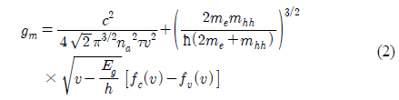
The material gain coefficient is described by a wideband steady-state numerical model [19]:

where
Each SOA is identical and characterized by a length of 900 μm, an active-layer width of 1.2 μm, an active-layer thickness of 0.1 μm, a confinement factor of 0.2, a bias current of 300 mA, an active-region refractive index of 3.2, a cladding refractive index of 3.0, and a carrier lifetime of 40 ps. To our knowledge, the only assumption we have made is the neglect of polarization issues. As is well-known, the polarization states of signals at the inputs of an SOA-MZI must be carefully controlled to achieve optimal performance. In a practical setup, a slight deviation of the optimum polarization states of the input signals would give rise to a reduction in the output power and device efficiency or performance, but there is no influence on the adder operation.
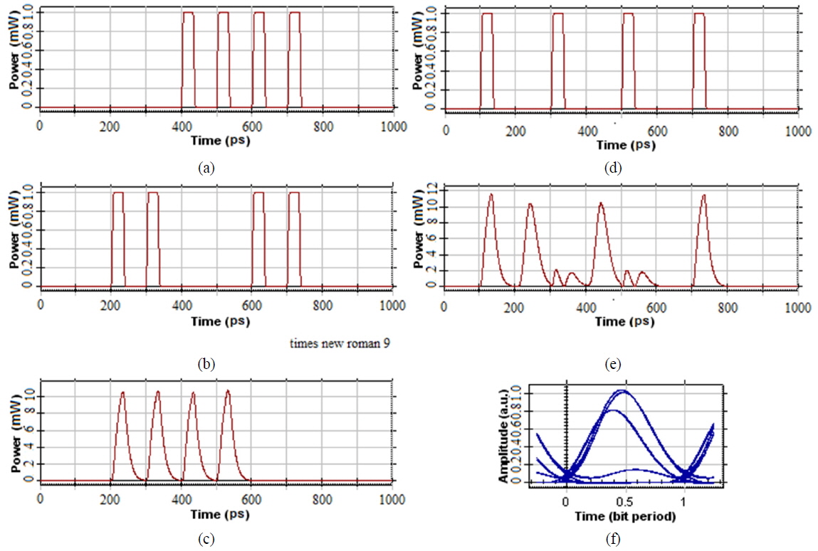
Simulation timing diagrams of the all-optical binary full adder for Sum output are shown in Fig. 3. The input signals A, B, and C are RZ modulated with a duty cycle of 33% at 10 Gb/s. Two optical input data signals A and B at wavelengths of 1553.32 (λ1) (193.0 THz) and 1552.52 nm (λ2) (193.1 THz) respectively, are applied to XOR Gate 1, which is realized using an SOA-based MZI. A CW control signal at wavelength 1550.92 nm (λ4) with a power of 0.5 mW acts as a third input to the SOA-MZI. The input data signals A and B with a peak power of 1 mW before entering the XOR Gate 1 are shown in Figs. 3(a) and (b) respectively. XOR Gate 1 output at a wavelength of 1550.92 nm (λ4) is shown in Fig. 3(c).
The simulation results of Fig. 3(c) show a high extinction ratio (values higher than 15 dB) for the signal at the output of XOR Gate 1. The main reason for this high performance is that the “zero/off” level is almost perfect, due to the destructive interference of the bias power and the two data-signal pulses in their respective SOAs at the output of the SOA-MZI during the period of occurrence of the 7th and 8th input optical data-signal pulses.
Figure 3(d) shows the input carry signal C at a wavelength of 1550.12 nm (λ3) with a peak power of 1 mW. The input carry signal C and output of XOR Gate 1 act as input signals to XOR Gate 2, which uses a CW signal at a wavelength of 1551.72 nm (λ5) as the control signal. The Sum output signal generated from the logic XOR operation at a wavelength of 1551.72 nm (λ5) and its corresponding eye diagram are shown in Figures 3(e) and (f) respectively. We observe some small residual pulses in the output, where ideally they should not appear. The extinction ratio of the Sum output signal was found to be 10 dB. The reasons for the lower performance of the signal were noise accumulation and the lower extinction ratio of the pulses used for switching XOR Gate 2.
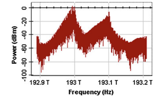
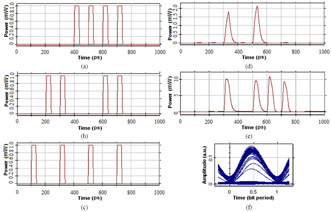
Input and output waveforms corresponding to the Carry output are shown in Fig. 4. The input data signals A and B with a peak power of 1 mW before entering the AND Gate 1 are shown in Figs. 4(a) and (b) respectively. Input data signals A (193.0 THz) and B (193.1 THz) interact in SOA3, thus generating the power at new FWM frequencies of 192.9 and 193.2 THz respectively. Figure 5 shows the spectrum at the SOA3 output. The conjugated light generated at 193.2 THz (1,551.72 nm) is filtered by OBF3. The AND output has a low power level, due to the low conversion efficiency of the FWM, and is therefore amplified before being applied in the next stage.
Figure 4(c) shows the input carry signal C at a wavelength of 1550.12 nm (λ3) (193.4 THz) with a peak power of 1 mW. The output of XOR Gate 1 at a wavelength of 1550.92 nm (λ4) (193.3 THz) and input carry signal C are applied to AND Gate 2. The conjugated light generated at 1551.72 nm (193.2 THz) is filtered by OBF4. In the logical AND operation, the conjugated light has a frequency close to that of the data signal, so a narrow OBF (0.32 nm) is selected for this purpose.
The output of AND Gate 2, representing the logical AND operation (A XOR B) C between the two inputs, is shown in Fig. 4(d). The outputs of AND Gate 1 and AND Gate 2 at a wavelength of 1551.72 nm (λ5) are logically ORed to produce the Carry output at the same wavelength. The Carry output signal generated from the logical OR operation at a wavelength of 1551.72 nm (λ5) and its corresponding eye diagram are shown in Figs. 4(e) and (f), respectively.
The maximum extinction ratio observed for the Carry output signal is 12 dB. The Carry output signal exhibits a lower extinction ratio due to the nonideal logical AND operations obtained through SOA-based FWM.
We present a new and potentially integrable scheme to realize an all-optical binary full adder, consisting of optical gates based on the nonlinear properties of a semiconductor optical amplifier. The circuit exploits two XOR gates, two AND gates, and one OR gate to obtain the Sum as well as the Carry output signal. Proof-of-principle operation is numerically evaluated at 10 Gb/s using return-to-zero data patterns. In our proposed design we achieve extinction ratios for Sum and Carry output signals of 10 dB and 12 dB respectively, which are more than adequate for all-optical logic-based information processing. The all-optical binary full adder can be a basic building block for more complex all-optical circuits.