For front contacts, the Ag-paste screen-printing technique has occupied most of the photovoltaic (PV) industry because the process is simple and easily automated, since it was first applied to solar cells in 1975 [1]. However, because Ag is expensive and has disadvantages such as low aspect ratio and high contact resistance, new metallization techniques have been researched [2]. For a new front contact, low contact resistance and good adhesion with an inexpensive material is required to make better-performing solar cells. To meet these requirements, Ni/Cu plating has been researched as a promising technique [2-4]. A nickel layer between copper and silicon acts as a good diffusion barrier, and also form nickel silicide, which yields low contact resistance and good adhesion after sintering [5].
Electroless nickel plating is a suitable method for solar cells after selective laser ablation of SiNx, as nickel can be plated by a self-aligned process on the opened narrow area [2]. Because electroless plating is a completely chemical process, bath conditions such as pH, temperature, and concentration can make a difference in the deposition properties [3]. For the deposition of metal, adhesive and surface coverage are significant characteristics. To meet the needs for these characteristics, the cluster size of deposited nickel is an important factor, and it depends on bath temperature and pH [6].
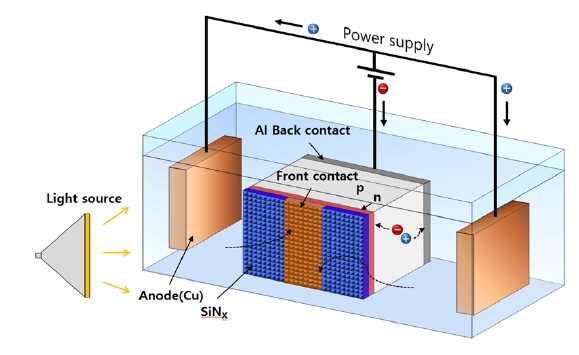
Above the nickel barrier layer, copper is deposited by light-induced electroplating (LIP) as the front contact thickening. LIP uses photocurrent, which is generated under light, and this has some advantages. A simplified process is possible because there is no need to contact the front side. Also, LIP can produce homogeneous plating compared to electroplating, because the front contact area has the same electrical potential over the whole area [7].
In this study, the pH and temperature of a nickel electroless plating bath are varied to investigate their influence on the adhesion of a Ni/Cu front contact.
Samples were prepared on a POCl3 diffused (70 ohm/sq) and pyramid textured
2.1. Nickel Electroless Plating
Ni plating was carried out by submerging the samples in an alkaline solution. Before nickel electroless plating, native oxide on the silicon area was etched using a 2% HF solution. Nickel chloride (NiCl2·6 H2O) was used as the main source. Each source was used for its own purpose: sodium hypophosphite (NaH2PO2·H2O) as a reducing agent, triammonium citrate ((NH4)3C6H5O7) as a complex agent, and ammonium chloride (NH4Cl) as a buffer agent to stabilize the pH of the solution. Also, ammonium hydroxide (NH4OH) was used to control the pH of the solution. The chemical reactions of nickel electroless plating are as follows [8-11]:


The net reaction in Eq. (3) is obtained by adding Eq. (1) and (2) for reactions that occur concurrently. The pH of the bath was varied as 8, 8.5, and 9 at 60 ℃; temperature was varied as 60, 70, and 80 ℃ in a bath of pH 8. To investigate the effect of sintering on contact adhesion, another nickel-plated sample with pH 8 was plated at 80 ℃. The sintering process was conducted in ambient N2 gas for 90 seconds at 300 ℃ in a conventional tube furnace, as nickel silicide (NiSix) can be formed between 200 and 900 ℃ [12].
Cu plating was conducted by light-induced plating. The main source of Cu is copper sulfate (CuSO4·5 H2O), which produces copper ions (Cu2+) in the bath. High copper concentration produces high current density in the solution. However, if copper from the anode contributes to exceed the solubility limit of 240 g/L, copper sulfate recrystallizes on the plating bath. Also, sulfuric acid (H2SO4) was added to the solution to enhance conductivity [13].


The above equations show the reaction at the anode (3), in the solution (4), and at the cathode (5). Figure 2 shows the Cu LIP process.
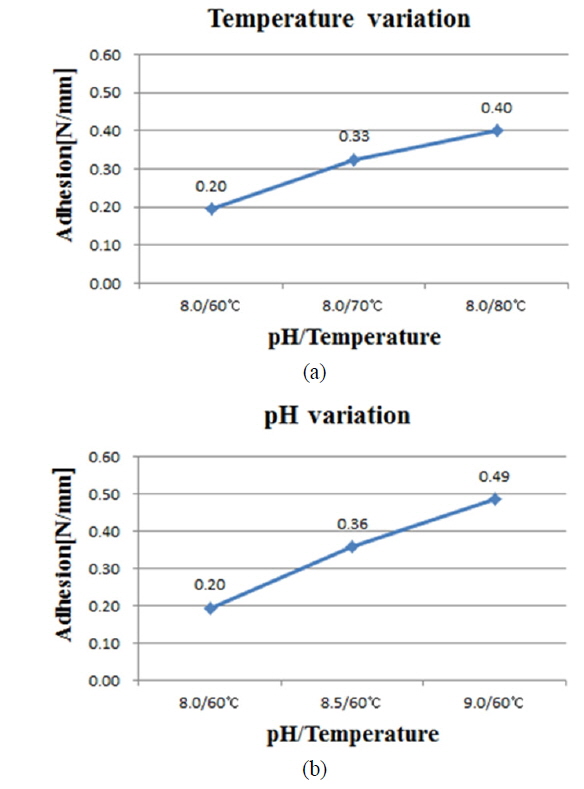
The peel force test was carried out using a UTM (H5KT) to see the influence of bath conditions on Ni/Cu contact adhesion. The measured nickel thickness was in the range of 400-500 nm, while the copper layer was about 4 ㎛ thick. The average adhesion was measured for a bus bar of length 64 mm and width 1.5 mm, for each pH and temperature value. The average adhesion values of non-sintered samples are plotted in Fig. 3, varying from 0.2 to 0.49 N/mm. The maximum adhesion strength value of 2.18 N/mm was recorded for pH 9 at 60 ℃ (even with no sintering process).
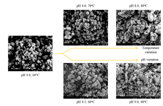
To study the dependence of nickel cluster size on various bath conditions, nickel layers were deposited for 2 minutes. Figure 4 shows FE-SEM top views of the nickel surface for various bath conditions (temperature 60-80 ℃, pH 8-9). A very slight change in cluster size was observed (170-200 nm) for each process condition. However, measuring the distinctive cluster sizes at each condition and identifying the expected variation in sizes were quite difficult due to the inconsistent cluster sizes, which depended on location: cluster size was different on a pyramid than in a valley.
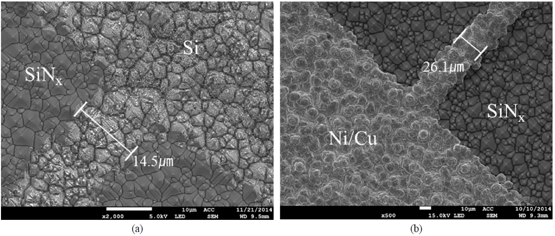
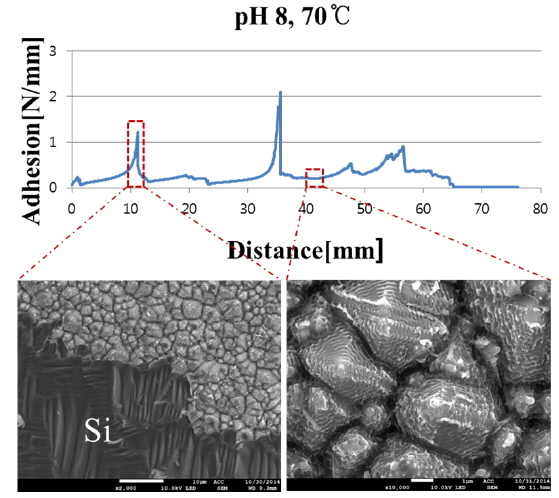
The sample that was nickel-plated at pH 8 and 70 ℃ was further investigated by comparing its adhesion result with its FE-SEM visual image. In Fig. 5, the peel force test results, along with FE-SEM top views of the silicon bus bar area, for the conducted peel force test sample are shown. It can be observed very clearly that the silicon material with high adhesion force is peeled off from the substrate along the Ni/Cu contact, while it is not affected in a low adhesion area. The adhesion strength difference was observed 6 to 10 times using areas with low and high adhesion results.
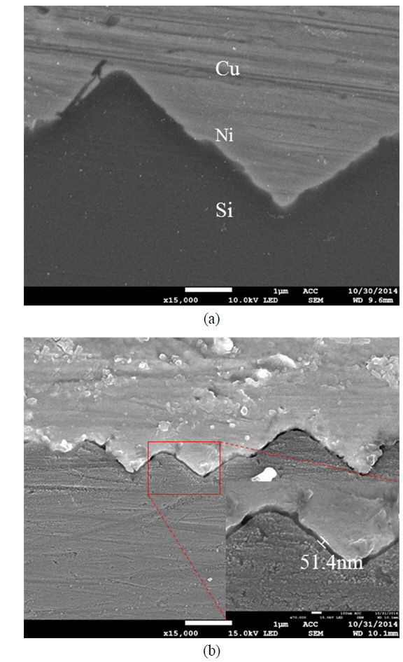
The non-sintered samples were further studied to confirm the formation of nickel silicide (NiSix) at the nickel-silicon interface. Selective nickel silicide etching was performed to check for a NiSix layer in the nickel-silicon interface using a solution containing 5% HF and 3% H2O2. The admixed solution of HF and H2O2 has already been reported to etch a NiSix layer selectively [14]. The images in Fig. 6 (a) and (b) show the FE-SEM cross sections of samples with no NiSix etching and NiSix etched samples respectively. The cross section in Fig. 6 (b) clearly shows that a NiSix layer about 50 to 100 nm in thickness was etched under the nickel layer, confirming the presence of a NiSix layer at the nickel-silicon interface. A possible reason for the presence of a NiSix layer, even with no sintering process, is the ribbon soldering process conducted at 390 ℃, as NiSix forms between 200 and 900 ℃ [2].
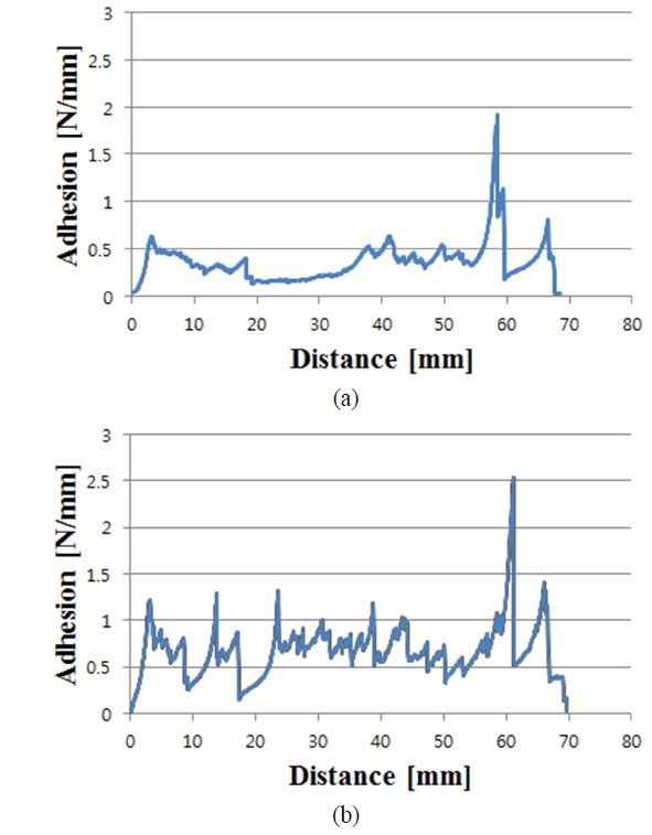
To see the influence of NiSix on the Ni/Cu contact adhesion, for the nickel-plated sample formed at pH 8 and 80 ℃ and sintered at 300 ℃ for 90 seconds, the peel force test was conducted and is shown in Fig. 7 (b). Figure 7 shows peel force test results for sintered and non-sintered samples. It can be seen that the overall adhesion values have increased for the sintered sample (Fig. 7 (b)), compared to the non-sintered sample (Fig. 7 (a)). The average adhesion value was improved about 1.8 times and the maximum adhesion strength of about 2.54 N/mm was recorded. The comparison of sintered and non-sintered samples using peel force test results is summarized in Table 1.
[TABLE 1.] Measured peel force test result of non-sintered sample and sintered sample
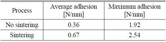
Measured peel force test result of non-sintered sample and sintered sample
Ni/Cu metal stacks were successfully deposited on laser-ablated ARC-opened silicon surfaces to form front electrodes for silicon solar cells. This experiment was carried out to study the effect of nickel cluster size on the adhesion of a Ni/Cu contact to a silicon surface. An average adhesion force of 0.2-0.49 N/mm, with a maximum value of 2.18 N/mm, was achieved without sintering. A slight change in cluster size, up to 30 nm, was detected for all values of pH and temperature. The high adhesion force of 2.18 N/mm is due to the ribbon soldering process for the peel force test. The presence of NiSix layers was confirmed by a selective NiSix etching process. By including the Ni sintering process, the average adhesion value was improved about 1.8 times, with a maximum value of about 2.54 N/mm being achieved. The sample with higher adhesion suggests that the formation of the NiSix layer is more critical than the Ni cluster size, varied by the bath conditions, for creating an adhesive Ni/Cu front contact on the silicon surface.