Liquid crystal displays (LCDs) are used widely in everyday life because of their various advantages such as light weight, low driving voltage, and low power consumption. Various efforts have been made to improve the quality of LCDs-for example, high transmittance, high resolution, high contrast, and wide viewing angle characteristics. Several liquid crystal (LC) modes, such as twisted nematic, vertical alignment, and in-plane switching (IPS), have been competing against one another in the LCD market [1-4].
Among the various LCD modes, the IPS mode is one of the mainstream technologies developed to achieve a wide viewing angle [4-9]. The IPS mode exhibits wide viewing angle characteristics because the LCs are rotated in a plane parallel to the glass substrates. However, the IPS mode suffers from low transmittance above the patterned electrodes.
To enhance the transmittance of the IPS mode, the fringe-field switching (FFS) mode has been proposed [10-13]. The FFS mode exhibits higher transmittance than the IPS mode. Moreover, an FFS cell using LCs with negative dielectric anisotropy (n-LCs) exhibits higher transmittance than one using LCs with positive dielectric anisotropy (p-LCs). In addition, n-LCs can be driven at a low frame rate, because image flickering due to the flexoelectric effect is smaller in n-LCs than in p-LCs [14]. However, the transmittance above and between the patterned electrodes in an FFS cell using n-LCs still needs further improvement. Moreover, the response time of n-LCs is longer than that of p-LCs because of the higher viscosity of the former. Several methods have been proposed to improve the transmittance and response time of the FFS and IPS modes [15-17]. However, these methods suffer from disadvantages such as complicated operation and high operating voltage.
In this paper, we propose an n-LC cell with parallel patterned electrodes for high transmittance and fast response. The proposed cell has a higher transmittance and a shorter response time than a conventional FFS cell using n-LCs, because the proposed cell does not have transmittance dips and has a thinner LC layer. It maintains the wide viewing angle characteristics of the conventional FFS mode using n-LCs.
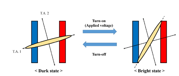
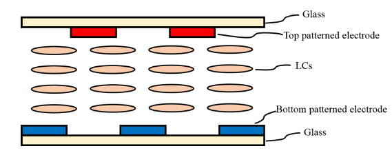
To improve the electro-optical characteristics of a homogeneously aligned n-LC cell, we employed a double-sided patterned electrode structure [17-21], as shown in Fig. 1. The top and bottom patterned electrodes were parallel to each other, but their positions were shifted away from each other.
Figure 2 illustrates schematically the operating principle of the proposed cell. The operating principle of the proposed cell is similar to that of the conventional FFS mode using n-LCs. In the initial state, the LCs are homogeneously aligned along one of the transmission axes of the crossed polarizers so that the cell is in the dark state. By applying different voltages to the top and bottom patterned electrodes, an oblique electric field is built into the LC layer. The LCs are rotated counterclockwise by the applied electric field, so that the proposed cell shows the bright state.
To confirm the electro-optical characteristics of the proposed cells, we used the commercial software TechWiz LCD 2D (Sanayi System Company, Ltd., Korea). The parameters used for numerical calculations were as follows. The width of the patterned electrodes and the gap between them were 2.5 μm and 3 μm, respectively. The LC material parameters used in simulations were:
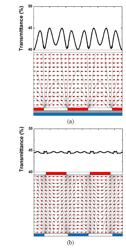
We compared the transmittance of the proposed cell to that of the conventional FFS mode using n-LCs. The thicknesses of the LC layer for maximum transmittance in the proposed cell and the conventional FFS mode were 2.3 μm and 2.45 μm respectively. The maximum transmittances of the proposed cell and the conventional FFS mode were 44.0% and 41.7% respectively. Figure 3 shows the transmittance distribution, potential profile, and LC director distribution of the conventional FFS mode and the proposed cell. As shown in Fig. 3, the transmittance distribution of the conventional FFS mode shows dips above and between the patterned electrodes; conversely, the transmittance of the proposed cell is nearly uniform. For this reason, the proposed cell demonstrated higher transmittance than the conventional FFS mode. In addition, the thickness of the LC layer for maximum transmittance of the proposed cell was smaller than that of the conventional FFS mode using n-LCs. In the conventional FFS mode, an electric field is applied between the patterned and common electrodes on the bottom substrate, so that the LC molecules far from the bottom substrate are not rotated. In the proposed cell, however, an electric field is applied between the top and bottom patterned electrodes, so that LC molecules everywhere can be rotated.
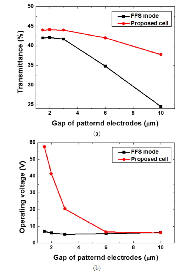
We compared the dependence of the transmittance on the gap between patterned electrodes. The birefringence of the n-LCs and the width of the patterned electrodes were 0.15 and 2.5 μm respectively. As shown in Fig. 4(a), the proposed cell shows higher transmittance than the conventional FFS mode under all conditions. In addition, as the gap between patterned electrodes increased, the operating voltage of the proposed cell decreased, as shown in Fig. 4(b).
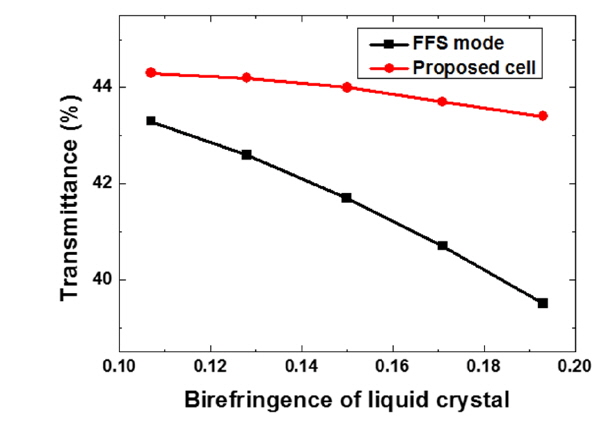
We compared the dependence of the transmittance on the birefringence of n-LCs. The thickness of the LC layer was chosen for maximum transmittance at each condition. The width of the patterned electrodes and the gap between them were 2.5 μm and 3 μm respectively. We assumed that all n-LCs have the same physical parameters except for the birefringence. As shown in Fig. 5, as the birefringence of the n-LCs increased the transmittance of the conventional FFS mode decreased, because the LC molecules above and between the patterned electrodes were not rotated for small cell gaps. However, the transmittance of the proposed cell was nearly the same for every condition.
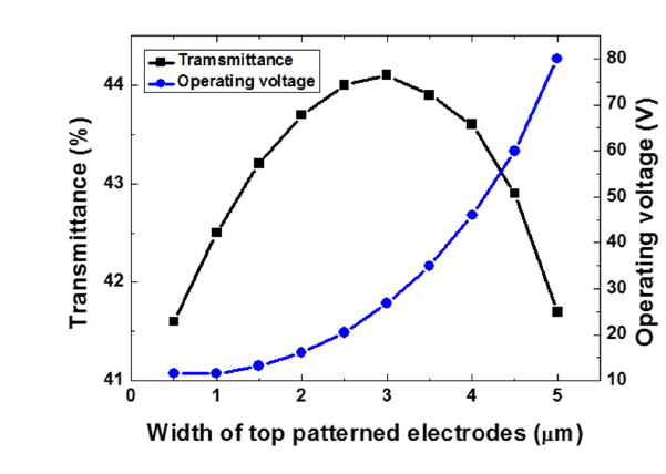
We compared the dependence of the electro-optical properties of the proposed cell on the width of the top patterned electrodes. The width of the bottom patterned electrodes and the gap between them were fixed at 2.5 μm and 3 μm respectively. The transmittance was maximized when the width of the top patterned electrodes was 3 μm, as shown in Fig. 6. As the width of the top patterned electrodes increased, the operating voltage increased, too.
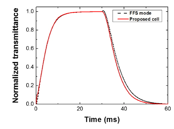
We compared the response time of the proposed cell to that of the conventional FFS mode, as shown in Fig. 7. The response time of the proposed cell was shorter than that of the conventional FFS mode. The turn-on times of the proposed cell and the conventional FFS mode were the same at 8.2 ms. The turn-off times of the proposed cell and the conventional FFS mode were 11 ms and 13.2 ms respectively. In the conventional FFS mode, LC molecules far from the bottom substrate were not rotated, because the electric field far from the bottom substrate was weak; conversely, in the proposed cell an electric field was applied between the top and bottom patterned electrodes, so that the LC molecules everywhere were rotated. Therefore, the proposed cell showed maximum transmittance at a smaller thickness of the LC layer than did the conventional FFS mode. When the proposed cell and the conventional FFS mode have the same cell gap of 2.3 μm, the turn-off times of the proposed cell and the conventional FFS mode were 11 ms and 11.6 ms respectively. Consequently, we can conclude that the difference in turn-off times between the two modes comes mainly from the cell-gap difference.
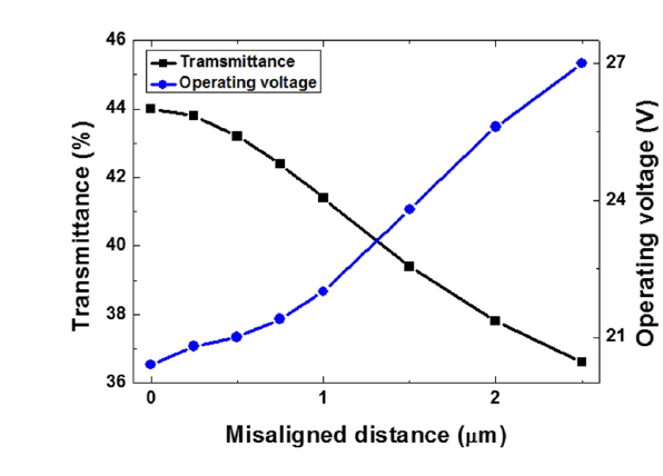
However, accurate alignment of the top and bottom patterned electrodes may be difficult in actual manufacturing processes. As shown in Fig. 8, the transmittance decreases and the operating voltage increases as the misalignment between the top and bottom patterned electrodes increases. When the misalignment is 1 μm, the transmittance of the proposed cell is 41.4 %, 5.9 % lower than that of the aligned cell. Therefore, precise alignment is required for high performance of the proposed cell.
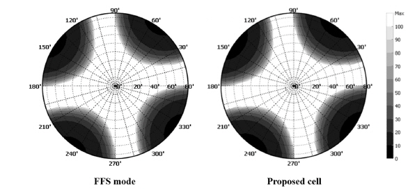
We calculated the iso-contrast distribution for the proposed cell and the conventional FFS mode. As shown in Fig. 9, the proposed cell exhibited wide viewing angle characteristics similar to those of the conventional FFS mode, because of the in-plane rotation of LC molecules.
In summary, we proposed an n-LC cell with parallel patterned electrodes for high transmittance and fast response. The proposed cell has shown higher transmittance than the conventional FFS mode using n-LCs, because the proposed cell does not have transmittance dips. In addition, the proposed cell has shown a shorter response time than the conventional FFS mode using n-LCs, because of smaller optimum thickness of the LC layer. In addition, the proposed cell exhibits wide viewing angle characteristics similar to those of the conventional FFS mode using n-LCs.