ZnO-based nanostructures have attracted much attention because of their exquisite sensitivity and fast response to the surrounding environment [1-5]. In recent years, n-type doping control of ZnO nanowires (NWs) has attracted great attention. Especially, ZnO-based NWs are particularly useful due to their manageable conductance with doping control in addition to their large length-to-diameter and surface-to-volume ratio versus bulk and films of ZnO [6]. The electrical conductivity of ZnO can change dramatically by the presence of reactive gases in the air; there have been many reports on the application of semiconducting metal oxides as gas sensors due to their small dimensions, low cost, and high compatibility with microelectronic processing[7,8]. Furthermore, ZnO-based semiconductor materials have received much attention due to their excellent electrical and optical characteristics, such as large band gap energy, of 3.37 eV, and large exciton binding energy, of 60 meV, at room temperature (RT) [9].
To date, in room temperature operation, most gas sensors still face difficulties in getting a high response to volatile organic chemicals (VOCs), such as ethanol, acetone, methanol, and LPG. Furthermore, there are few reports on the study of the gas-sensing properties of Ag-doped ZnO NW to ethanol. Some reports have shown possible room temperature operation for ethanol using ZnO NWs [10]. To obtain high responses and selectivity, different approaches, such as microstructure control, doping, and changing operating temperatures have been adopted to modify the sensing properties of semiconductor metal oxide gas sensors [11,12]. It is known that the sensing mechanism is based on the surface reaction of the nanostructure with the exposed gas (adsorption and desorption of the test gas molecules). As adsorption is a surface effect, one can increase the adsorption of gas molecules by decorating with nanoparticles or doping with an element that has a stronger chemical affinity for that particular gas molecule. Doping in a NW can create defects and these defects play a role as preferential adsorption sites for gas molecules, which can help to sense pollutant gases at lower temperatures [13].
In this study, ZnO nanowires, undoped and doped with 3 wt.% Ga, were grown using pulsed laser deposition in a furnace (PLDF) and nanowire gas sensors were fabricated. The sensitivity ranges of ethanol gas sensors varied depending on the amount of Ga dopant due to different carrier concentration in the ZnO NWs. The ethanol gas sensing properties of these materials were characterized using a self-assembled sensing analyzer. The effect of Ga content on gas sensing properties to ethanol for high sensitivity and high selectivity was investigated in detail. The sensing mechanism of the gas sensor to ethanol is also discussed.
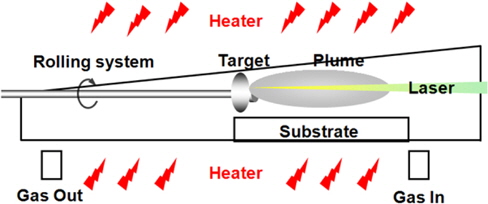
ZnO-based NWs were synthesized by a PLDF process on 20 Å Au film as a catalyst on sapphire substrates. The PLDF has a target rotating system, ensuring homogeneous target ablation. ZnO and 3GZO targets were used to fabricate the NWs under optimized conditions. The diverse ZnO-based NWs were grown in a PLDF at a temperature of 800℃ with Ar carrier gas (Fig. 1). During the deposition, the Ar gas flow rate was fixed at 90 sccm and the pressure inside the quartz tube was maintained at 1.2 Torr. A KrF excimer laser (248 nm), operating at a pulse repetition rate of 10 Hz, was focused on to a pristine ZnO target for the growth. The energy density of the laser was set to 1.2 J/cm2, and the shot area on the target surface was 0.042 cm2. The morphology of asgrown samples was studied by field emission scanning electron microscopy (FE-SEM), operated at 20 kV. Energy-dispersive X-ray spectroscopy (EDX) analysis of a single NW was conducted to analyze the chemical composition of the doped NWs. The growth time of the ZnO-based NWs was 30 min.
For the fabrication of the ZnO-based sensors, we spread out NWs on Si substrates after cleaning. Soon after photolithography, the substrates were developed. For the ohmic contact, metal electrodes, consisting of Ti (20 nm) and Au (150 nm), were deposited by e-beam/thermal evaporator and patterned by a liftoff process to form contact pads on NWs. The sensitivity of the module was measured with the concentration of the ethanol gas at 1 ppm in the self-designed gas chamber at 300℃.
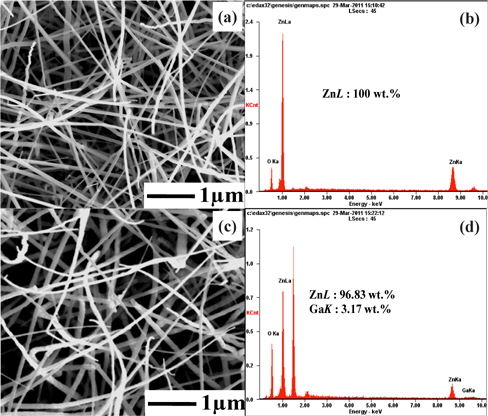
Figures 2(a-d) show the controlled morphology of the ZnO and 3GZO NWs and EDX spectra. SEM with EDX (SEM/EDX) is an electron probe microanalysis method that has been used extensively to characterize the size, morphology, and elemental composition of samples. The NWs have thread-like shapes and a Au nanoparticle at its end is clearly observed. It is understood that the nanoparticle is an Au catalyst that initiates the growth of the NWs by HWPLD, one of the vapor-liquid-solid (VLS) mechanisms. The catalyst can be identified based on the fact that the tips are brighter than the stem parts of the NWs. As can be seen in the figure, the orientation and the distribution of the NWs are random, with a diameter of ~100 nm and the length of ~1 μm. ZnO-based NWs were synthesized with ZnO targets by PLDF. Figures 2(a) and (c) show the top view of FE-SEM images of ZnObased NWs with pure ZnO and 3GZO with a 20 Å Au film as a catalyst. As shown in Fig. 2, many random-direction ZnO-based NWs with a mean diameter of ~70 nm and an average length of ~9 μm were obtained at 800℃.
The EDX analysis yielded reasonably accurate quantitative results featuring all the elements present in the test compounds: C, O, N, Na, S, Al, Si, and Cl. Furthermore, the carbon film has a very low backscattered electron (BSE) yield compared with that from the particles. Thus, in BSE mode, the particle image can be observed with very high contrast. This improves quality and speed of the automated mapping of particles by SEM prior to EDX analysis [4]. Figure 2 shows a backscatter electron image of the morphology and surface composition of the fractured surface of a specimen, which corresponds to the EDX spectrum. It can be seen that there is a clear ZnO and Ga-related peak with some unidentified peaks at 1.5 and 2.0 keV, probably from the substrate. The EDX spectrum revealed the presence of Zn and Ga elements. PLDF is a well-established growth method for oxide thin films and nanostructures of high structural quality. Thus, PLDF is a simple synthesis process and only target control can give effective doping in the ZnO NWs. Such a result indicates that the impurities were doped well in the ZnO-based NWs.
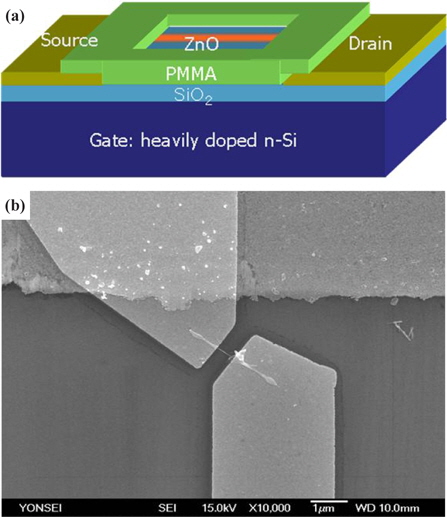
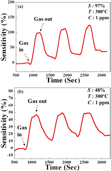
It is important to realize highly functional NW-field effect transistor (FET) devices for the optimization of sensing properties. NW-FETs also have many advantages to enhance the sensitivity and selectivity for different gas species. It has been reported that ZnO NW-FET show remarkable n-type FET characteristics [14,15]. The transport properties of our single NW-FET device exhibited excellent n-type characteristics with strong gate control. The NW-FET sensors shown in Figure 3 were used for the detection of ethanol gas at 300℃. The system was purged with N2 gas to remove excess oxygen species from the surface of the NW in the chamber. The sensitivity of the ZnO and 3GZO NWs sensor for 1 ppm at 300℃ ethanol gas is shown in Fig. 4. The sensitivity, defined as (Rg−Ra)/Ra, where Rg and Ra is the electrical resistance in ethanol gas and dry air, respectively, changes with different dopants in ZnO-based nanowire FETs. The sensitivities of the sensors were 97% and 48% for ZnO, and 3GZO, respectively. The main effects of doping in oxide semiconducting NWs are the changes in electronic conductivity and the introduction of defects into the NWs. These factors play important roles in changing the sensitivity in NW sensors. Defects within the crystal structure can improve the adsorption of gas molecules on the NW surface and the change in the conductivity will change the position of the Fermi level in the energy band diagram, which governs the electronic transportation between gas molecule and NW material [16].
If ZnO NW was doped with the same quantity, it would be different in resistance. The resistance of GZO might be more conductive than ZnO, due to a difference in the quantity of carriers. Thus, sensitivity can also be changed proportionally to the formula of the sensitivity’s definition. In fact, oxygen adsorption plays an important role in the electrical properties of the doped ZnO nanomaterial with microstructures. Oxygen ion adsorption removes the conduction electrons and increases the resistance of ZnO. Reactive oxygen species, such as O2−, O2− and O− are adsorbed on the ZnO surface at elevated temperature, and the amounts of such chemisorbed oxygen species depend strongly on temperature. At low temperatures, O2− is chemisorbed, while at high temperatures, O2− and O− are chemisorbed, and the O2− disappears rapidly. The whole of the oxygen adsorption process can be described by the following formulae [17]:


In addition, the electrical detection of any chemical species is dependent on the surface reactions between the NWs and the chemical molecules. The ethanol sensing mechanism of this ZnO-based gas sensor can be described as follows: [18]

The sensitivity and sensing window of ZnO-based NW gas sensors can be expanded by different doping in the NWs. The ZnObased nanowires were fabricated using a self-designed PLDF instrument to compare the sensing functions with various impurities. The conductivity and ethanol gas sensitivity of the sensors doped with different impurities were investigated. In the case of the undoped ZnO and the 3GZO NW gas sensor, measured sensitivities were 97% and 48%, when the sensor was operated at 300℃ with 1 ppm of ethanol gas. The response time and recovery time were also fair. Consequently, we can easily control the sensitivity for the same gas by using different concentrations of Ga and selectivity is also expected to change with doping materials. The sensitivity ranges of ethanol gas sensors could be expanded depending on the amount of Ga dopant due to the control of different carrier concentration in the ZnO NWs.
In summary, the sensitivity and sensing window of ZnO-based NW gas sensors can be expanded by different doping in the NWs. The ZnO-based nanowires were fabricated using a self-designed PLDF instrument to compare the sensing functions with various impurities. The conductivity and ethanol gas sensitivity of the sensors doped with different impurities were investigated. In the case of undoped ZnO and the 3GZO NW gas sensor, measured sensitivities were 97% and 48% when the sensor was operated at 300℃ with 1 ppm of ethanol gas. The response time and recovery time were also fair. Consequently, we can easily control the sensitivity for the same gas by using different concentrations of Ga and selectivity is also expected to change with doping materials.
A plausible explanation on the improved sensing behavior in the doped NWs compared to undoped NWs is related to the defects created by doping. Doping in NWs can generate defects, such as oxygen vacancies, metal interstitials, and surface defects, and these defects play a vital role in the sensing of ethanol gas. The obtained dependencies of the sensitivity for differently doped ZnO NW-based sensors are discussed considering the undoped and Ga-doped. Experimental data confirm the prospects of thin ZnO NWs as active elements for nanoscale sensors operating at room temperature. The sensing mechanisms of ZnO NWs were determined. These results demonstrate that ZnO NWs can be used as a gas-sensing material for fabricating highly sensitive gas sensors and are expected to find wide applications in various complex moist gases for the quick detection of poisonous and inflammable gases.