Recently, ZnO-based oxide materials, such as amorphous indium gallium Zinc Oxide (a-IGZO), have attracted much attention as channel materials in TFTs used for driving and switching devices such as active matrix organic light-emitting diodes (AMOLED) and active matrix liquid crystal displays (AMLCD). TFTs exhibit excellent characteristics, including, for example, a high field-effect mobility (> 10 cm2V−1s1), a large on/off current ratio (107~108), a low fabrication temperature, good uniformity, and high optical transparency [1-3]. Although a-IGZO TFTs have such desirable properties, the instability of their threshold voltage (VTH) under illumination with light can be a critical obstacle for their use in displays because the devices are exposed to ambient light during operation. Recently, several studies have reported on the VTH instability under a negative bias and under illumination stress (NBIS), and the results can be summarized into three models where the degradation is caused by (1) light-induced oxygen interstitial generation [4]; (2) trapping of a photo-generated hole [5,6]; and (3) an ionization oxygen vacancy [7-9].
However, the detailed role of light in NBIS degradation has not yet been clearly presented.
In this paper, the degradation caused by light stress (LS) in a-IGZO TFTs is investigated. In order to elucidate the influence of light, the VTH instability is measured and compared under LS without applying a voltage bias, positive gate bias stress (PBS), negative gate bias stress (NBS), positive gate bias illumination stress (PBIS), and NBIS. For these materials to be used in transparent devices and displays, the presence of visible light is important. The wavelength (λ) for LS is fixed to 532 nm, assuming that in real applications, ultraviolet radiation with λ = 430 nm or below can be blocked by proper UV-absorbing coatings. The oxygen flow rate is differentiated during IGZO deposition to control the concentration of native defects in the active layer.
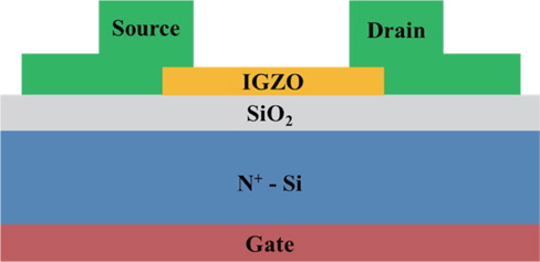
a-IGZO TFTs with an inverted and staggered structure were fabricated on an n+-silicon substrate. After growing a 120-nm gate dielectric on thermal SiO2, an active 50-nm a-IGZO layer was deposited via RF magnetron sputtering at room temperature using a target of In2O3: Ga2O3:ZnO = 2:2:7. The RF power and the partial pressure of the mixed Ar and O2 gases were maintained at 100 W and at 5 mTorr, respectively. Here, the O2 flow rate was applied at either 1 and 10 sccm while the Ar flow rate was fixed at 30 sccm. After the active patterning was completed through a wet etching process, the post-deposition annealing (PDA) was carried out in an O2 ambient at 300℃ for 1 h. Then, the source/drain electrodes (Ti) and the backside gate electrodes (Al) were formed via RF magnetron sputtering. Finally, the a-IGZO TFTs were annealed in a forming gas ambient at 400℃ for 30 min. The TFTs measured 100 by 100 μm2 (W×L), and the constant current method was used to extract VTH, with VTH defined as the bias of gate voltage that forces the drain current to (W/L) × 1 nA at VD = 0.1 V. The schematic cross-section of the a-IGZO TFT structure is shown in Figure 1.
The electrical characteristics of the a-IGZO TFTs were measured using an Agilent 4155B semiconductor parameter analyzer. For the LS, the laser (λ=532 nm) was illuminated onto an a-IGZO TFT channel with a light intensity of 0.2 W/cm2.
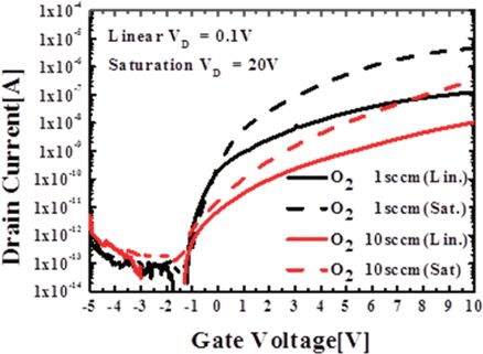
Figure 2 presents the results of the I-V measurement for the a-IGZO TFTs that were fabricated. The electrical parameters were recorded at the room temperature, as shown in Table 1. When the oxygen flow rate was lower, VTH shifts to a more negative direction and the sub-threshold slope (SS) decreases from 1.25 to 0.5 V/decade. The decrease in the oxygen flow rate is well known to lead to a high number of oxygen vacancies suppressing the interstitial formation of oxygen [12]. Considering that oxygen vacancies are the source of free carriers in ZnO-based TFTs with zinc interstitials [10,11], the changes in the I-V characteristics resulting from adjustments to the oxygen flow rate can be explained by the concentration of free carriers and defects.
[Table 1.] Electrical properties of a-IGZO TFTs with different oxygen flow rates.
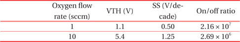
Electrical properties of a-IGZO TFTs with different oxygen flow rates.
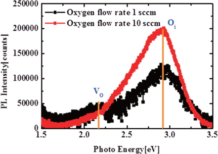
To confirm that the oxygen flow rate had an effect on the concentration of the defects, we analyzed the RT PL spectra of the a-IGZO film layer, as shown in Figure 3. Two peaks are observed at 2.1~2.3 eV and 2.7~2.9 eV. The peak at 2.1~2.3 eV is related to the recombination between oxygen vacancies and the valence band [13]. The peak at 2.7~2.9 eV is related to the recombination between oxygen interstitial and the valence band [13,14]. The RT PL spectra indicate that a lower oxygen flow rate causes more oxygen vacancies and less oxygen interstitial.
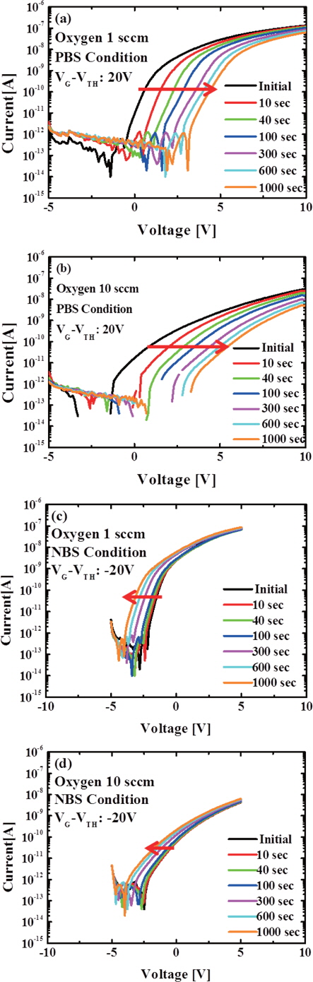
Figures 4(a) and (b) shows the I-V characteristics under PBS with a constant gate bias voltage of 20 V for 1,000 sec. The shifts in VTH are observed to be in the positive direction as the gate-bias stress time increases, without a degradation in the SS.
The parallel-shifted transfer characteristics have been explained by free-electron charge trapping at/near the gate dielectric/ channel [15-17]. The device with an oxygen flow rate of 10 sccm reveals a larger shift in VTH, which can be explained by the fact that a-IGZO TFTs with a higher oxygen flow rate have a higher density in interstitial oxygen traps in the interface at/near the gate dielectric/channel [12]. Figures 4(c) and (d) show the I-V properties under NBS with a constant gate bias voltage of −20 V for 1,000 sec. VTH shifts toward the negative direction as the time of the gate bias stress increases, without degradation in the SS. These results are also explained by the free hole trapping mechanism [17-19]. The amount of shift in the VTH under NBS is noticeably smaller than that under PBS. This is because a-IGZO is an n-type material with native defects such as oxygen vacancies and zinc interstitial [20-22], and there are negligible holes in the valance band [18].
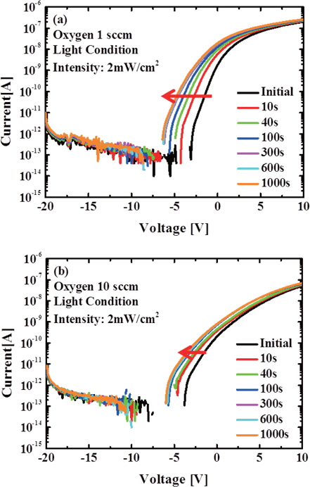
Figure 5 shows the results of the I-V measurement under LS for 1,000 sec without a gate bias stress. Illumination with light causes a considerable negative shift in VTH with a slow recovery characteristic, as reported in previous studies. These observations have been explained through three models, as mentioned before.
In the light-induced oxygen interstitials model, light breaks down the zinc-oxygen bonds, and broken oxygen atoms diffuse to interstitial sites, simultaneously forming an oxygen vacancy. The induced oxygen interstitial acts as a donor in a-IGZO TFTs. When the LS is removed, the induced oxygen interstitial diffuses back to the oxygen vacancy sites, recovering its initial state. However, the diffusing oxygen atoms must overcome the potential barriers surrounding the atom, and therefore, a-IGZO TFTs have a slow recovery characteristic [4]. In this model, however, a high-energy light, such as UV or with a wavelength (λ) < 420 nm, is required for the generation of interstitial oxygen. So, the light-induced oxygen interstitial model is not proper in our experiment where λ=532 nm.
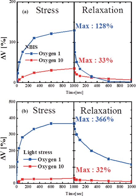
In the case of the trapping of photo-generated holes where the oxygen interstitial is excited through illumination, generating free hole carriers, the free hole carriers are trapped in the interface at/near the gate dielectric/channel and show slow recovery characteristics because the potential energy barriers to the initial state for the trapping holes are not negligible. In this experiment where there is no gate bias, however, the hole trapping localized in the interface at/near the gate dielectric/channel is not dominant. Moreover, if the mechanism for trapping a photo-generated hole is followed, the device with a higher oxygen flow rate reveals a greater VTH shift because the a-IGZO TFTs with a higher oxygen flow rates have a higher trap density of oxygen interstitial [12]. However, in Figure 6, the devices with an oxygen flow rate of 10 sccm show a smaller shift in VTH than those with an oxygen flow rate of 1 sccm.
In the ionization oxygen vacancy (VO) model for the LS instability, neutral oxygen vacancies (VO0) are transformed to double ionization oxygen vacancies (VO2+) under illumination, and photo-generated electrons increase the conductivity in the channel [7-9]. The enhanced conductivity is known to be persistent because the state transforming from VO2+ to VO0 requires a large amount of energy to change the electron configuration.
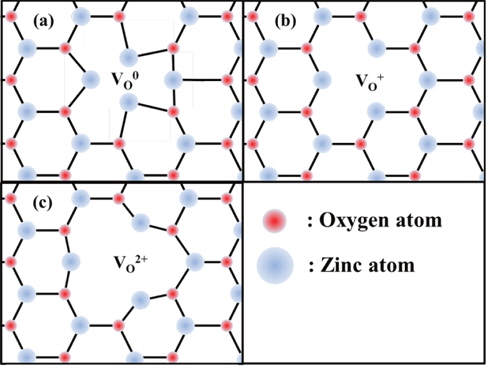
Figure 7 shows the electron configuration of oxygen vacancies with different ionization conditions. In a zinc atom with a neutral state, inward relaxation occurs strongly toward oxygen vacancies, and in a +1 charge state, the zinc atom was inwardly relaxed, slightly toward the oxygen vacancy. In a +2 charge state, the zinc atom was outwardly relaxed, strongly against the oxygen vacancy [20-24]. As a result of the large differences in the electron configuration, the VO site has negative-U center characteristics. That is, the neutral and double state oxygen vacancies are more stable [20-22]. If the ionization oxygen vacancy mechanism is followed, the device with a lower oxygen flow rate reveals a greater shift in VTH than under LS because the lower oxygen flow rate induces more oxygen vacancies, which is consistent with the experimental results. Based on the ionization VO model, PBIS and NBIS are analyzed in order to interpret the illumination effects on the instability of VTH.
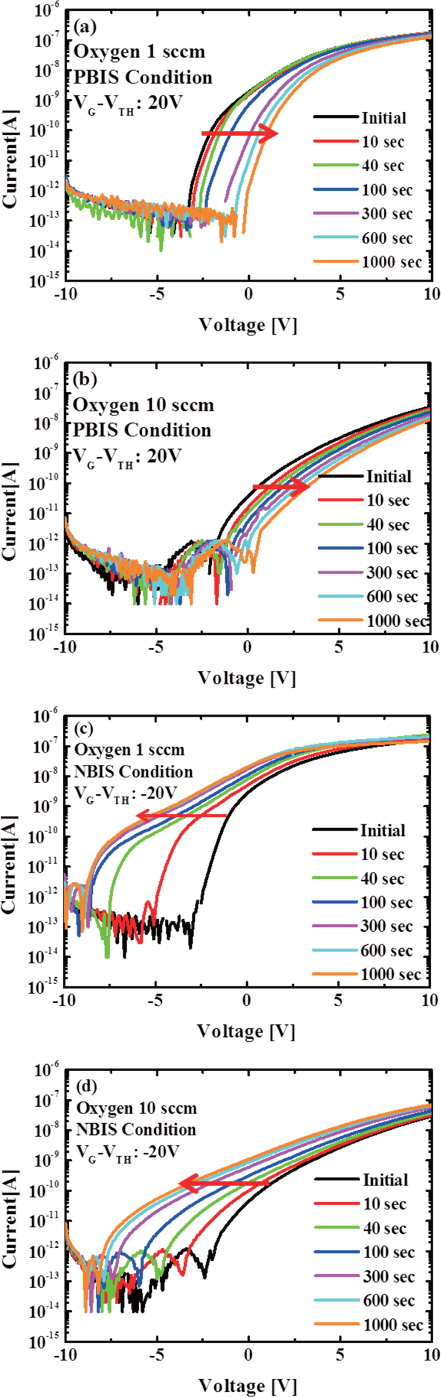
Figures 8 (a) and (b) show the transfer characteristics of the a-IGZO TFTs after PBIS at VGS= 20 V with illumination for 1,000 sec. The shifts in the VTH were observed to be in the positive direction, similar to PBS but a VTH shift that was much smaller. The explanation is that in in PBIS, electrons are generated by transforming VO0 to VO2+ by photons, which is countervailed by electron trapping at/near the gate dielectric/channel. Dominance is dependent on the amount of oxygen vacancies and on the trap density. Figures 8(c) and (d) shows the I-V characteristics of a-IGZO TFTs after NBIS at VGS = −20 V with illumination for 1,000 sec. There is a negative VTH shift similar to NBS but the VTH shift is much more than under NBS. This is because the enhanced conductivity is accelerated by photo-generated hole trapping due to the gate bias. In this experiment, the oxygen flow rate was altered in order to control the oxygen vacancies, and the observations are in agreement with the ionization oxygen vacancy model in which an oxygen flow rate of 1 sccm shows a larger VTH shift under PBIS and NBIS.
In this paper, we investigated the instability of VTH under visible light illumination of RF sputtered a-IGZO TFTs with different oxygen flow rates. The RT PL analysis shows that the device with an oxygen flow rate of 1 sccm has a higher VO concentration than 1 sccm. After PBS and PBIS, a positive shift in VTH was observed, but the shift in VTH under PBIS was smaller than that under PBS. In NBS and NBIS, the negative shift in VTH appears, but VTH shifts under NBIS more than under NBS. Moreover, in each case, the device with an oxygen flow rate of 1 sccm showed a larger shift in VTH than with 10 sccm. These results indicate that the origin of the LS-induced instability in VTH is the VO site in the a-IGZO TFTs channel layer.