A Simple Model for a DGS Microstrip Line with Stepped Impedance Slot-Lines
- Author: Woo Duk-Jae, Lee Taek-Kyung, Nam Sangwook
- Publish: Journal of electromagnetic engineering and science Volume 15, Issue1, p26~30, 00 Jan 2015
-
ABSTRACT
In this paper, a simple equivalent circuit model for a defected ground structure (DGS) microstrip line with stepped impedance slot-lines in the ground plane is presented. In addition, an analytic expression for the resonance frequency of the proposed structure is derived. In equivalent circuit modeling, the capacitance and the inductance of the resonance circuit are evaluated from the dimensions of the etched pattern in the ground plane. The resonance frequencies calculated from the proposed method are compared with those obtained with an electromagnetic (EM) simulation.
-
KEYWORD
DGS , Equivalent Circuit Model , Stepped Impedance Slot-Line
-
The planar transmission line with a spiral-shaped defect in the ground plane is one of the most popular slot-shaped defected ground structures (DGSs) [1]. Based on this structure, several modified slot-shaped DGSs have been proposed to comply with required performances [2-8]. In terms of circuit modeling, many other researchers have presented equivalent circuits for various slot-shaped DGSs. Simple lumped elements circuit models [8,9] and geometric models based on transmission lines were proposed in [10-13]. These efforts have provided improved physical insight into the operation principle of the DGS.
The stepped impedance resonator (SIR) is used in the filter design in order to push the spurious pass-band to a higher frequency range [14,15] and to reduce the circuit size [16]. In addition, this resonator has become very popular in the design of dual-band filters since the dual pass-band behavior can easily control the second pass-band [17].
In this paper, we describe the dual-band property of the microstrip line with a stepped impedance slot-line DGS in the ground plane. This paper also proposes an equivalent circuit model that provides insight into the coupling mechanism between the microstrip line and the stepped impedance slot-line, as well as a technique for obtaining analytic expression of the resonance frequencies.
II. CIRCUIT MODEL AND RESONANCE PROPERTIES
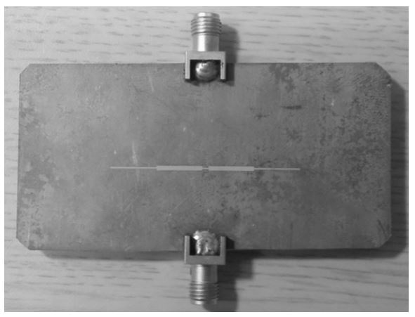
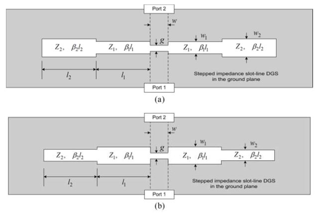
The configurations of the proposed stepped impedance slotline DGS on the ground plane of the microstrip line are shown in Fig. 1, where two short-circuited stepped impedance slotlines with different characteristic impedances Z1 and Z2 and electrical lengths
θ 1(=β 1l 1) andθ 2(β 2l 2) are connected by a narrow etched gap. In the DGS, the narrow etched gap can be modeled as a quasi-static capacitance [18]. The transmission line model for the etched pattern on the ground plane is shown in Fig. 2(a), in which two stepped impedance slot-lines are short-ended and are connected in parallel with a gap capacitance of 2Cs . In order for the etched pattern in the ground pla-ne to operate as a resonant circuit, the input impedance Zin (=jXin ) of the stepped impedance slot-line must have an inductive reactance as
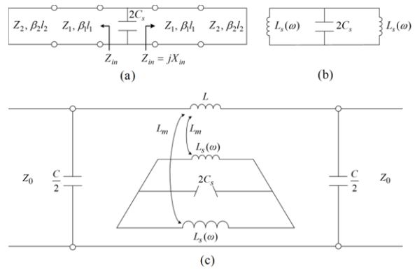
The transmission line model of the stepped impedance slot-lines is replaced by an equivalent circuit as depicted Fig. 2(b), where the equivalent inductance is
Here,
c is the speed of light, andεe1 andεe2 represent the effective permittivity of the first and the second slot-lines, respectively.
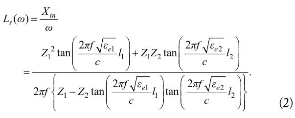
Based on the equivalent resonance model of the etched pattern on the ground plane, the equivalent circuit model of the microstrip line with stepped impedance slot-line DGS is shown in Fig. 2(c) [13]. The
L and theC are the inductance and the capacitance of the microstrip line corresponding to the length occupied by the DGS. The DGS on the ground plane is modeled as a parallel resonant circuit with inductanceLs(ω) and capacitanceCs that is coupled to the microstrip line through mutual inductance,Lm .
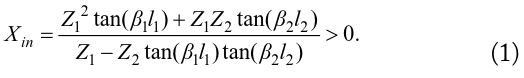
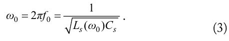
In the design of a DGS, it is important to find an analytic expression for the resonance frequency, which can be directly derived from the dimensions of the etched pattern. From Fig. 2(c), the resonance angular frequency is
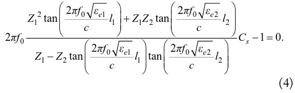
By substituting Eq. (2) for
Ls (ω 0) in Eq. (3), we can finally obtain the following expressionThe closed-form expression for the effective permittivity and the characteristic impedance of the slot-line were reported in [19]. The narrow etched gap on the ground plane can be modeled as a microstrip gap [18], and a closed-form expression for microstrip gap capacitance 2
Cs can be obtained from [11]. With the help of MATLAB, we can calculate the fundamental resonance frequency and the spurious resonance frequencies from Eq. (4).
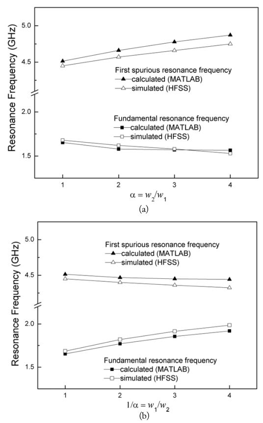
For the proposed structure, it would be of interest to see how the fundamental resonance frequency (
fr ) and the first spurious resonance frequency (fs 1) change as the slot width ratio (ω 2/ω 1) and the slot length ratio (l 2/l 1) are modified. To simplify the proposed structure, we chose the slot-line lengthsl 1 =l 2 = 12 mm.For the dimensions
l 1 =l 2 =12 mm and g = 0.3 mm, the fundamental resonance frequencies, the first spurious resonance frequencies, and the normalized first spurious resonance frequencies (η =fs 1/fr ) of the proposed structure are calculated for the changes in the slot-line width, and are summarized in Table 1. In the design, a circuit board RO3010 with a dielectric constant of 10.2, copper thickness of 0.016 mm, and substrate thickness of 1.27 mm is used. The characteristic impedance of the microstrip line is designed to be 50 Ω (ω = 1.2 mm). When the width of the first slot-line is fixed asω 1 = 0.3 mm, the normalized first spurious resonance frequencyη increases as the width of the second slot-line (ω 2) grows. In addition, for the fixed width of the second slot-line withω 2 = 0.3 mm, it is confirmed that the calculated normalized first spurious resonance frequencyη decreases as the width of the first slot-line grows. From the results in Table 1, it becomes evident that the normalized first spurious resonance frequencies can be controlled by the width ratio (slot impedance ratio), and this is the special feature of the SIR [17].We compared the predicted results of the proposed model with the EM simulated results. The simulation was performed using EM software HFSS version 11 (ANSYS Inc., Canonsburg, PA, USA). The resonance frequencies and the first spurious resonance frequencies from the proposed model and those from EM simulation are plotted in Fig. 3 as the slot width ratio changes. In the proposed circuit model, we ignored the influence of the step and short discontinuities in the slot-line, since no analytical results are available for various slot-line discontinuities. The discrepancies may be attributed to these factors. However, the predicted results of the proposed model agree with the EM simulated results.
Fig. 4 illustrates the comparative
S -parameters from the EM simulation (HFSS) and the measurement of a fabricated DGS with the dimensionsl 1 =l 2 = 9 mm,ω 1 = 0.9 mm,ω 2 = 0.3 mm, andg = 0.3 mm (Fig. 5). The characteristic impedance of the microstrip line is designed to be 50 Ω (ω = 1.2 mm). The normalized first spurious resonance frequencies obtained from the EM simulation and the measurement are 2.32 and 2.23, respectively.This paper has presented an analytical expression for the resonance frequencies and the equivalent circuit model of a DGS with stepped impedance slot-lines in the ground plane of the microstrip line. The theoretical prediction was in reasonable quantitative agreement with the EM simulated resonance property.
-
[Fig. 1.] Configurations of the microstrip line with a stepped impedance slot-line defected ground structure (DGS) in the ground plane. (a) ω1 < ω2. (b) ω1 > ω2.
-
[Fig. 2.] (a) Short-ended slot-line model and (b) equivalent inductance model for the etched pattern in the ground plane. (c) Lumped element equivalent circuit model for a microstrip line with stepped impedance slot-lines.
-
[]
-
[]
-
[]
-
[]
-
[Table 1.] 
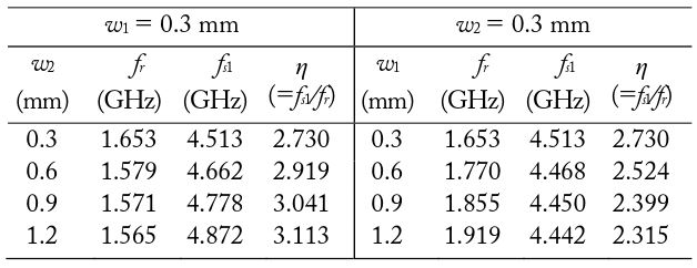
Calculated fundamental resonance frequencies, first spurious resonance frequencies, and normalized first spurious resonance frequencies for various slot widths (l1 = l2 = 12 mm)
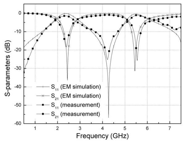
-
[Fig. 3.] Comparative resonance frequencies between EM simulation and calculation. (a) ω1 is fixed at 0.3 mm. (b) ω2 is fixed at 0.3 mm.
-
[Fig. 4.] S-parameters from the EM simulation and the measurement.
-
[Fig. 5.] View of the bottom of the fabricated defected ground structure.