검색 전체 메뉴
PDF
맨 위로
OA 학술지
Optimization of a Defected Ground Structure to Improve Electromagnetic Bandgap Performance
  • 비영리 CC BY-NC
  • 비영리 CC BY-NC
ABSTRACT
Optimization of a Defected Ground Structure to Improve Electromagnetic Bandgap Performance
KEYWORD
Defected Ground Structure (DGS) , Dispersion Analysis , Electromagnetic Bandgap (EBG) , Power/Ground Noise
  • I. INTRODUCTION

    In high-speed printed circuit boards (PCBs), the propagation of power/ground (P/G) noise causes a significant degradation of signal integrity. Today, data rates are continuously increasing, so noise coupling through the P/G planes occurs over a wide range of frequencies. Therefore, wideband suppression of P/G noise coupling is an essential requirement for high-speed PCBs. Electromagnetic bandgap (EBG) structures have emerged as an effective solution because they have wide stopband bandwidths, high stopband attenuation, and are easily integrated with PCBs [1]. Various techniques have been proposed to improve the noise-suppression characteristics while minimizing the size of EBG structures; these include the use of high dielectric constant materials, multivia structures, cascaded EBG cells, and defected ground structures (DGSs) [1]. The employment of DGSs has a distinctive advantage over the other methods: design modifications (i.e., removing a part of a ground plane) add no cost.

    In [2], circular DGS patterns are proposed for further improvement of the stopband bandwidth with a smaller perforation area. An analytical model is also presented to determine the bandgap characteristics of the proposed structure. The method proposed in the present study involves the segmentation of a transmission line with an arbitrary characteristic impedance into multiple sections so that the characteristic impedance can be regarded as a linear function of x (the wave propagation axis) in each section (i.e., applying the piecewise linear approximation). Good model-hardware correlation and flexible simulation setups allow us to explore a variety of DGS shapes in order to determine the best DGS pattern for maximizing the stopband bandwidth.

    II. OPTIMIZATION OF DGS SHAPES

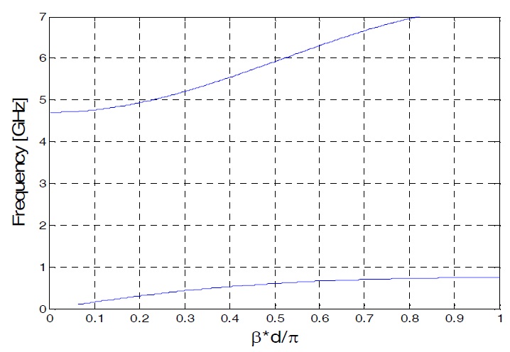
    The proposed analytical method considers two lower quasi-TEM modes and estimates the start and stop bandgap frequencies (fL, fH) with reasonable accuracy when compared to fullwave simulations. The proposed method allows rapid analysis of various DGS shapes at the early stages of the design process.

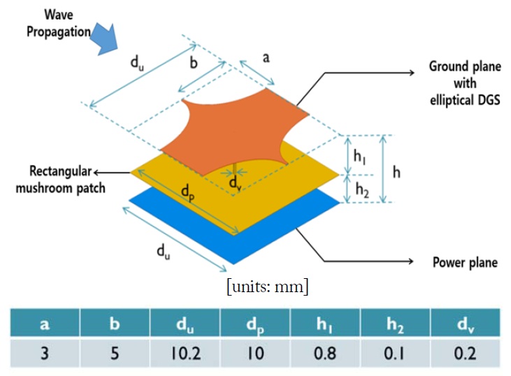
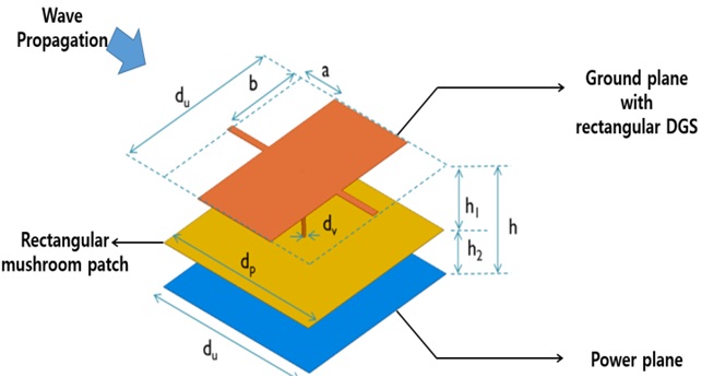
    Fig. 1 shows a mushroom-type EBG structure with elliptical DGS patterns. It consists of three metal layers: a dedicated power plane (bottom), EBG patches (middle), and an elliptical DGS (top). An FR-4 substrate is used as a dielectric material (εr = 4.4, tanδ = 0.02). Fig. 2 shows a dispersion diagram calculated using the proposed method, and the stopband ranges from 0.75 to 4.71 GHz. Fig. 3 shows a full-wave simulation result of the same elliptical DGS (Fig. 1). The stopband (–30 dB suppression level) ranges from 0.70 to 3.95 GHz. The proposed method analyzes a unit cell using the periodic boundary conditions (i.e., assuming an infinite array), whereas the full-wave simulation model is made of 3×7 unit cells. Compared with a circular DGS, the elliptical DGS (not yet optimized) has a slightly improved suppression bandwidth.

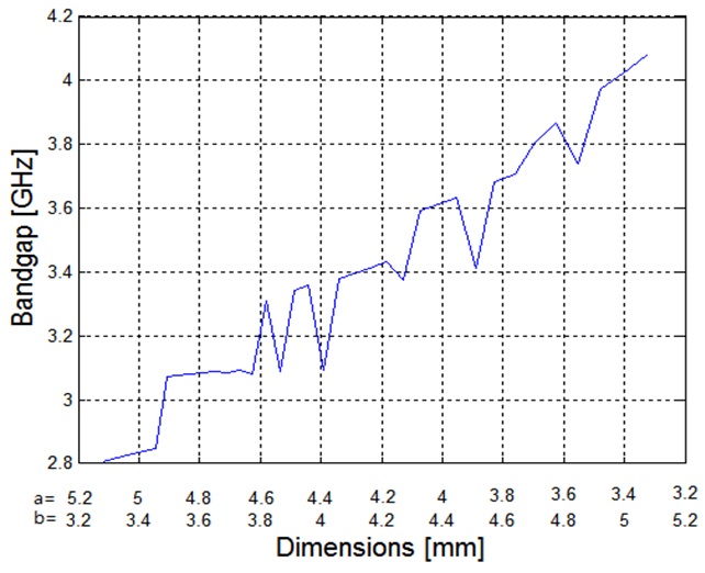
    Next, the dimensions (a and b in Fig. 1) of the elliptical DGS are changed such that its perforation area remains the same [units: mm] Fig. 1. Unit cell for an electromagnetic bandgap with elliptical defected ground structure (DGS) patterns. Fig. 2. Dispersion diagram of the structure shown in Fig. 1. (50%). In Fig. 4, the stopband bandwidth widens as b increases and a decreases. In other words, for a fixed perforation area, aligning the major axis of an ellipse perpendicular to a noisepropagating direction is advantageous.

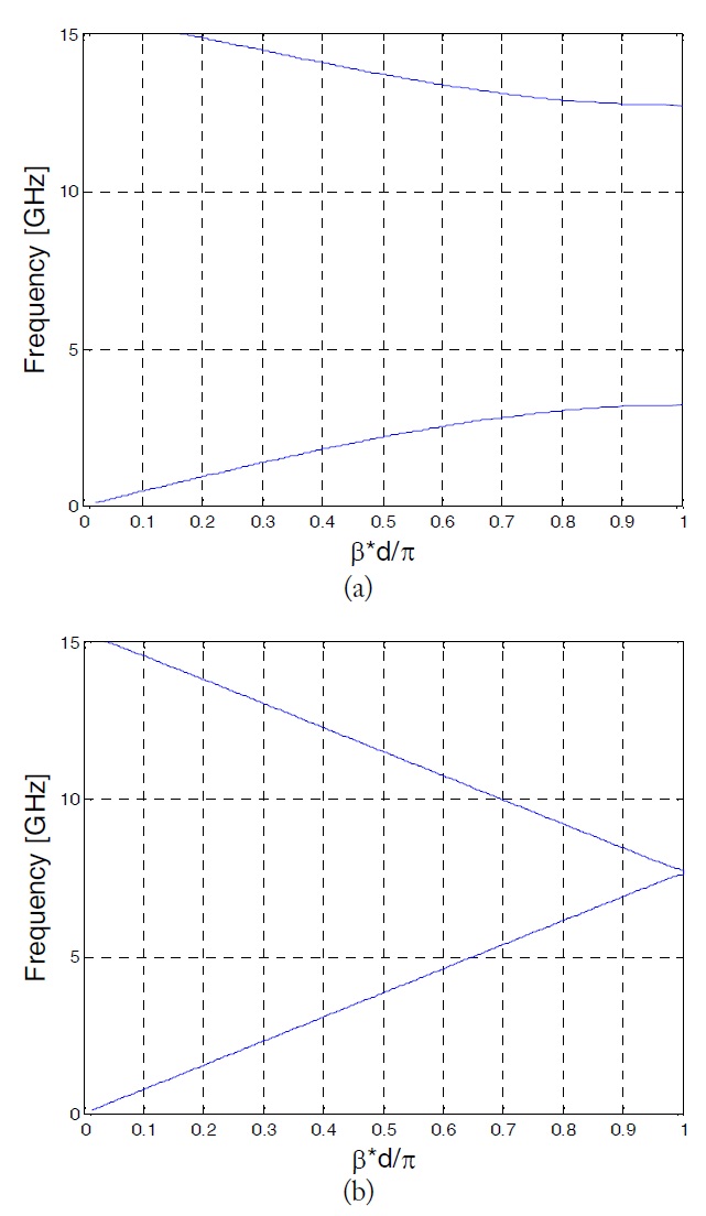
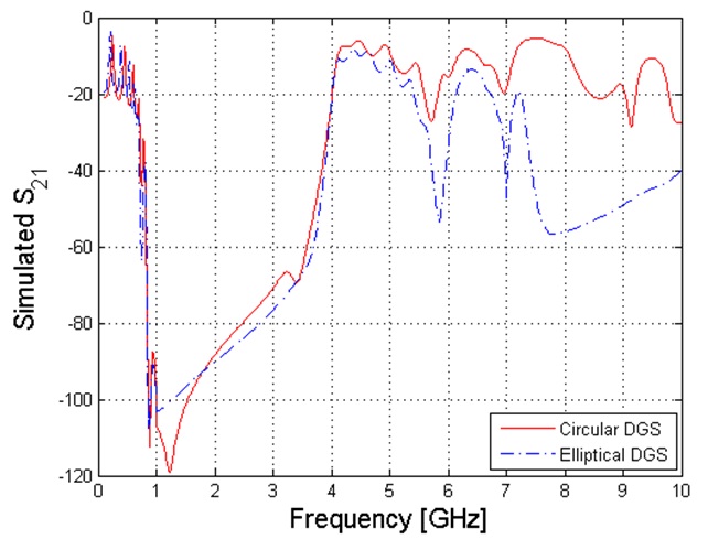
    Two rectangular DGS patterns are then compared to determine whether the same principle applies to other DGS shapes, as shown in Figs. 5 and 6: one with a = 2.5 mm and b = 5 mm, and the other with a = 5 mm and b = 2.5 mm. The other dimensions remain the same as in Fig. 1. The first shape has a stopband from 3.14 to 12.71 GHz, while the second has an almost zero stopband. Again, the longer side of a rectangle should be placed perpendicular to the noise-propagating direction.

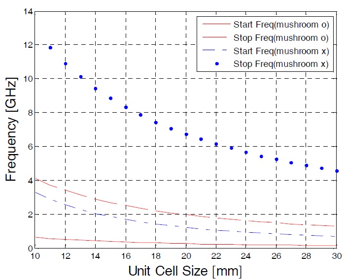
    Next, we change the unit cell size (du), maximize b (b = du / 2 – 0.1), and determine a, such that the perforation area remains 50%. Fig. 7 shows that fL, fH, and the stopband bandwidth all decrease as the unit cell becomes larger. An EBG without a mushroom-type patch has much higher fL and fH, but the tendency remains the same. Filling a given EBG area with more pieces of a smaller unit cell is advantageous. This also improves periodicity, so that the stopband characteristics are closer to the ideal case. Note that the dispersion analysis assumes that an infinite number of EBG cells are placed.

    III. CONCLUSION

    We extend the analytical method presented in [2] to explore a variety of DGS shapes in the search for better stopband characteristics. The data presented here do not necessarily represent the optimum achievable bandgap performance for each DGS pattern; however, the analysis procedure provides a basis for numerical optimization techniques that can be used in synthesizing DGS shapes that will meet existing bandgap requirements and layout constraints.

참고문헌
  • 1. Kim M., Koo K., Hwang C., Shim Y., Kim J., Kim J. 2012 "A compact and wideband electromagnetic bandgap structure using a defected ground structure for power/ground noise suppression in multilayer packages and PCBs," [IEEE Transactions on Electromagnetic Compatibility] Vol.54 P.689-695 google cross ref
  • 2. Kim M., Kam D. G. 2014 "A wideband and compact EBG structure with a circular defected ground structure," [Transactions on Components, Packaging and Manufacturing Technology] Vol.4 P.496-503 google
이미지 / 테이블
  • [ Fig. 1. ]  Unit cell for an electromagnetic bandgap with elliptical defected ground structure (DGS) patterns.
    Unit cell for an electromagnetic bandgap with elliptical defected ground structure (DGS) patterns.
  • [ Fig. 2. ]  Dispersion diagram of the structure shown in Fig. 1.
    Dispersion diagram of the structure shown in Fig. 1.
  • [ Fig. 3. ]  Influence of defected ground structure (DGS) shape variation on bandgap width.
    Influence of defected ground structure (DGS) shape variation on bandgap width.
  • [ Fig. 4. ]  Influence of defected ground structure shape variation on bandgap width.
    Influence of defected ground structure shape variation on bandgap width.
  • [ Fig. 5. ]  Unit cell for an electromagnetic bandgap with rectangular defected ground structure (DGS) patterns.
    Unit cell for an electromagnetic bandgap with rectangular defected ground structure (DGS) patterns.
  • [ Fig. 6. ]  Dispersion diagram of the structure shown in Fig. 5: (a) a = 2.5 mm, b = 5 mm, and (b) a = 5 mm, b = 2.5 mm.
    Dispersion diagram of the structure shown in Fig. 5: (a) a = 2.5 mm, b = 5 mm, and (b) a = 5 mm, b = 2.5 mm.
  • [ Fig. 7. ]  Effect of unit cell size on start and stop bandgap frequencies.
    Effect of unit cell size on start and stop bandgap frequencies.
(우)06579 서울시 서초구 반포대로 201(반포동)
Tel. 02-537-6389 | Fax. 02-590-0571 | 문의 : oak2014@korea.kr
Copyright(c) National Library of Korea. All rights reserved.