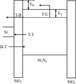
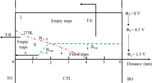
Charge Trap Flash (CTF) memory devices, otherwise known as metal-oxide-nitride-oxide-silicon structures, have been the subject of attention in the semiconductor industry due to their advantages over conventional floating gate type memory. These advantages include lower programming voltage, superior programming/erasing speeds, and a simple fabrication process compatible with standard complementary metal-oxidesemiconductor technology [1-3]. Recently, CTF memory devices have gained increasing interest in the three dimensional (3D) integration for next generation nonvolatile memory technology [4,5]. The tunnel oxide thickness plays a crucial role in regulating the erasing speed, data retention characteristics and charge loss mechanisms for CTF memory devices [6], while the thickness of the nitride charge trapping layer is less critical. Nevertheless, in 3D architectures, the nitride thickness has a direct effect on charge storage performance and array density [7]. Moreover, temperatures [8] and trap energy levels [9,10] also are considerable factors for understanding the electron loss mechanisms. Hence, in this letter, Pt/Al2O3/Si3N4/SiO2/Si (MANOS) charge trapping memory capacitors with various thicknesses of nitride layer were fabricated. We investigated and analyzed the effect of nitride thickness, trap energy levels and temperatures on electrons loss behavior in the retention state for MANOS capacitors. Also, a reasonable nitride thickness range was obtained through electrical characteristic measurements. Four charge loss mechanisms [11,12] are involved in the data retention state for scaled CTF memory devices: trapped electrons tunnel from traps to the silicon conduction band (T-B), trapped electrons tunnel from traps to the Si/SiO2 interface traps state (T-T), holes tunnel from the silicon valence band to nitride traps (B-T) and thermal excited trapped electrons from the traps to the nitride conduction band followed by tunneling through the tunnel oxide (T-E), as shown in Fig. 1. However, the T-B and T-E mechanisms are regarded as the two main electron loss mechanisms [11]. Therefore, in our case we only consider the T-B tunneling and T-E mechanisms.
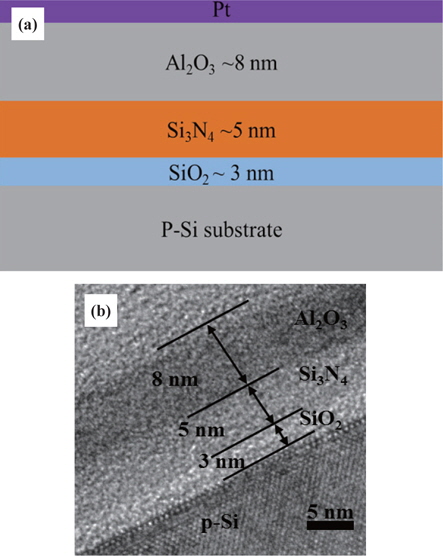
The MANOS capacitors were fabricated on p-type (100) Si substrates with a resistivity of 8-12 Ω·cm. Prior to deposition, the p-Si were cleaned by the standard radio corporation of America (RCA) process. Then, these substrates were dipped in HF solution for one minute to remove the native oxide. After a growth of thermal SiO2 tunnel oxide (TO) with a thickness of 3 nm in dry O2 ambience, the nitride (Si3N4) as charge trapping layers (CTL) ranging from 1 to 6 nm were deposited by low pressure chemical vapor deposition at 700℃. Subsequently, a 8 nm Al2O3 layer was deposited as the blocking oxide (BO) by atomic layer deposition (ALD) using trimethylaluminium (Al(CH3)3) precursor at a substrate temperature of 300℃. The thickness of the samples was measured by a spectroscopic ellipsometer and transmission electron microscopy (TEM). Finally, platinum (Pt) top electrodes with an area of 7.85×10⁻⁵ cm2 were deposited using magnetron sputtering at room temperature. Figures 2(a) and (b) show a schematic diagram and cross-sectional TEM image, respectively, of the charge trap flash memory device with a 5 nm Si3N4 CTL. The electrical characteristics of these memory capacitors were analyzed by a Keithley 4200 semiconductor characterization system.
In order to have a quantitative understanding of the electrons loss mechanisms in the data retention state, we have calculated the time constant associated with the T-B and T-E processes to characterize the electrons loss behavior. The time constant of T-B, τT-E, and the time constant of τT-E are written as [11]:


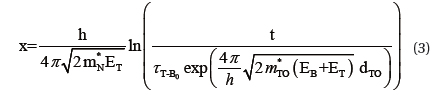
where τT-E is a time constant [13], = 0.42 m0 [14] and = 0.25 m0 [11] are the electron effective mass in the SiO2 and Si3N4, respectively, here m0 is the free electron mass. ET is the trap energy level referenced to the conduction band edge in the Si3N4 (eV), q is the absolute electron charge, EB=1.05 eV [15] is the energy barrier height of electron tunneling (eV), h is Planck’s constant, dTO is the thickness of the SiO2 (nm), T is the absolute temperature (K), A is the temperature independent constant, kB is Boltzmann’s constant, t is the retention time (s) and is the tunneling distance in the Si3N4 measured from the SiO2/Si3N4 interface as follows (nm):
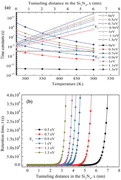
We assumed that the traps are spatially uniform inside the Si3N4 with an arbitrary energy level distribution, and all traps are initially filled with electrons in the retention state. The BO absolutely restricts electrons tunneling to and from the gate electrode. Fig. 3(a) shows the results of the calculated time constant based on Eqs. (1) and (2). For the electrons captured by shallow trap energy levels (ET≤ 0.5 eV), τT-E (<10-3 s) is at least 2 orders of magnitude smaller than τT-B, suggesting that T-E is a much quicker electrons loss path than T-B tunneling. These trap energy levels cannot effectively capture electrons due to their smalland have no contribution to electron retention. If > 0.5 eV, T-B tunneling starts to influence electrons loss and the the two electron loss mechanisms compete with each other. At 273 K, a relatively small τT-B for electrons trapped near the TO (x<1 nm) suggests that T-B tunneling plays a leading role in the electrons loss process of the region. However, increases to 6 nm, τT-B increases at least 10 orders of magnitude, and the deeper the trap depth, the larger the increase, indicating that T-B tunneling becomes more and more difficult, especially for those deep ET. Moreover, the electron loss path starts to change with increasing, and T-E gradually becomes the important electron loss mechanism from shallow ET to deep ET. It is worth noting that there is little effect of T-B tunneling on electron retention when x>4 nm. It was also found that τT-E decrease by several orders of magnitude when increasing the temperature, and more and more trapped electrons tend to be de-trapping through T-E, which is the dominant electron loss mechanism when the temperature exceeds 470 K. This means that the dominant region of T-B will gradually reduce to disappear with an increase of temperature from 273 to 500 K. Fig. 3(b) exhibits the tunneling distance of different ET in the retention state based on Eq. (3). It was observed that x decreases with ET increasing from 0.5 to 1.3 eV at the same retention time, indicating that the electrons trapped at deep ET are less affected by T-B tunneling.
Figure 4 illustrates how the two electron loss processes influences the retention state for MANOS devices. Ⅰ and Ⅱ represent the T-B and T-E dominant region at 273 K, respectively, and the boundary (marked by) is drawn on the basis of the above results. At a retention time t (e.g., 1,000 s), region Ⅰ and Ⅱ should contain empty traps and filled traps. As the electron loss process continues, the empty-filled traps boundary marked by BT-B and BT-E moves toward the BO side and the bottom of the Si3N4 band gap, correspondingly. The boundary of BⅠ / Ⅱ, which is nonlinear with tunneling distance, moves down at elevated temperatures, suggesting that T-E gradually dominates the electron loss process.
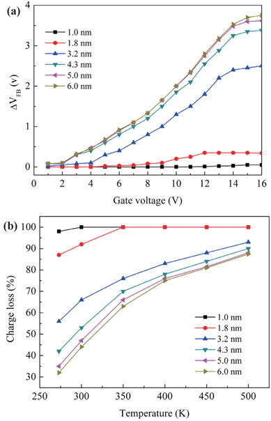
The memory window △VFB (flat-band voltage shift) extracted from the 1 MHz capacitance-voltage (C-V) curve under different program voltages is shown in Fig. 5(a). In the thickness range of our study, much smaller VFB of MANOS devices with an Si3N4 layer less than 3.2 nm are observed, indicating that injected electrons are not trapped effectively but are lost quickly. Though the program speed and memory window increase with a thick Si3N4 layer, the △VFB appears to be fairly similar when the thickness exceeds 4.3 nm. This result is ascribed to the reduced electric field through Si3N4 due to the increasing Si3N4 thickness, which gives rise to a decrease of electron trapping efficiency. The retention characteristics of the samples after 10 hours at different temperatures are shown in Fig. 5(b). It shows that high charge loss is observable for thin Si3N4 less than 3.2 nm even at 273 K. As illustrated in Fig. 3(a), the T-B tunneling dominates the electron loss process for thinner Si3N4 due to the small τT-B, and those trapped electrons near the TO/Si3N4 interface are lost quickly through the TO to the substrate. By increasing the thickness of Si3N4, the retention characteristics can be improved. However, at and above 4.3 nm, the charge loss is almost independent of Si3N4 thickness, especially for temperatures exceeding 470 K. These results can be attributed to the electron loss mechanisms transition between T-B and T-E, as illustrated in Fig.4. When T-E dominates the electron loss process, the retention characteristics are not affected by the gradual increase of Si3N4 thickness. Hence, in the thickness range of our study, we deduce that a Si3N4 thickness of more than 6 or less than 4.3 nm has no contribution to improving the memory performance.
In summary, we investigated the effect of nitride thickness, temperature and trap energy levels on the electrons loss behavior of a Pt/Al2O3/Si3N4/SiO2/Si CTF memory structure. In a data retention state, T-B and T-E tunneling compete with each other to influence the retention characteristics, even at 273 K. Those trapped electrons near TO (<1 nm) and at a shallow ET (<0.5 eV) inside the Si3N4 are lost quickly via T-B and T-E tunneling, respectively. With an increase of Si3N4 thickness and temperature, T-B tunneling is gradually reduced, while T-E dominates the electrons loss process. At a certain ET, electrons may adopt different loss paths, which depend on the Si3N4 thickness and temperature. The electrical measurement results demonstrate that a thin Si3N4 layer of less than 3.2 nm has no effective trapping ability. Though the storage performance can be improved by increasing Si3N4 thickness, the data retention characteristics are almost independent of nitride thickness at elevated temperatures, especially temperatures exceeding 470 K. The above results can pave a way for device design in the future.