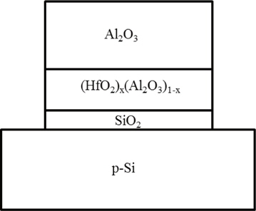
According to the 2012 International Technology Roadmap for Semiconductors (ITRS) [1], the conventional floating gate nonvolatile semiconductor memories (FG-NVSM) are approaching their scaling limitation; moreover, new materials and technology are required in order to explore the novel solid state nonvolatile memory device with the desired characteristics, such as the low-cost, high-density and a fast program/erase (P/E) speed for use in mobile electronics [2-5]. For conventional FG-NVSM devices, the charges are stored in a conducting poly-silicon gate, and a single defect in the tunneling layer can discharge the whole memory due to the scaling thickness of the tunneling layer. Based on the concept, that charges are stored in discrete traps within the charge trapping layer, silicon-oxide-nitrideoxide- silicon (SONOS) charge trap flash (CTF) memories with nitride (Si3N4), as the charge trapping layer, have attracted much attention for commercial applications in order to replace the conventional FG-NVSM devices due to lower operating voltage, excellent endurance, smaller size and compatibility with standard CMOS technology [6]. However, one problem in the SONOS memory device is the small conduction band offset between the Si3N4 and the tunneling layer [7], which leads to poor retention characteristics. In order to solve the problem, employing high-k dielectrics, as the charge trapping layer in the SONOS structure, has been reported by many researchers [8-14]. The charge memory structure with a pure HfO2 charge trapping layer demon-strates an excellent charge storage performance at low voltages, faster program speed and less over erase problems compared to conventional SONOS devices. However, such a memory device has poor data retention capability due to the crystallization of HfO2 film after high temperature annealing treatment [15]. In this paper, the SONOS type CTF memory capacitors with the (HfO2) x(A12O3)1-x charge trapping layer, SiO2 tunneling layer and Al2O3 blocking layer were fabricated; further, the schematic cross section structure was illustrated in Fig. 1. The effects of the charge trapping layer composition on the memory characteristics, such as memory window, retention characteristics, band alignment and trap energy levels, were reported.
Five types of memory capacitors were prepared in the experiment. Prior to memory capacitors fabrication, p-type Si (100) substrates with a resistivity of 3~20 Ω·cm were cleaned by the standard Radio Corporation of America (RCA) process in order to remove the native oxide. Next, 3 nm SiO2 film, as the tunneling layer, (TL) was thermally grown in dry O2 ambience. Subsequently, 10 nm (HfO2)x(A12O3)1-x (HAO) charge trapping layer (CTL) with various x values were deposited by atomic layer deposition (ALD) using HfCl4 and a trimethylaluminium (Al(CH3)3) precursor at a substrate temperature of 300℃. Al content in HAO films were controlled by adjusting the number of deposition cycles. Then, another 12 nm Al2O3 was deposited by ALD as the blocking layer (BL). The fabricated memory capacitors were rapid thermal annealed (RTA) at 800℃ for 30 s in N2 atmosphere. Finally, platinum (Pt) gate electrodes with an area of 7.85×10⁻⁵ cm2 were deposited on the heterojunction by using the magnetron sputtering technique at room temperature. Silver paste was spread on the back side of the Si substrate as the bottom electrodes. X-ray photoelectron spectroscopy (XPS) was used to investigate the atomic concentration of HAO films, band gap and band offsets of the memory capacitors. The electrical characteristics of the memory capacitors were measured using a Keithely 4200 semiconductor characterization system (4200 SCS) in the dc sweeping mode and pulse mode. In this case, the five memory capacitors are denoted as S1, S2, S3, S4, and S5, respectively, and their corresponding parameters are provided in Table 1.

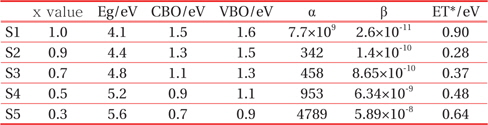
Corresponding parameters for five memory capacitors. x and Eg are HfO2 mole fraction value and band gap of HAO CTL, respectively. CBO and VBO represent the band offset between TL/CTL. α is a combination of the temperature independent constants, and ·is the extracted trap energy level maximum value at 200℃ after 105 s.
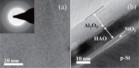
Figure 2 demonstrates the transmission electron microscopy (TEM) images of HAO films after RTA treatment. It is observed that the HAO film after RTA remained in the amorphous phase, as confirmed by the selected area electron diffraction (SAED) pattern in the inset of Fig. 2(a). Figure 2(b) is the cross section (TEM) image of the S2 sample, which conveys distinct interfaces of Si/SiO2, SiO2/HAO and HAO/Al2O3.
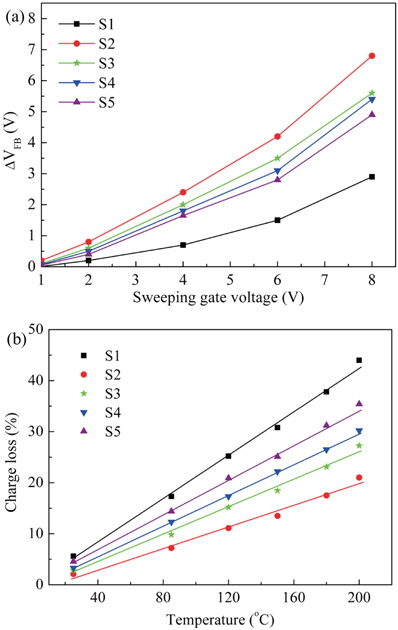
The memory windows, ΔVFB, named as flat-band voltage shift, can be extracted from the 1 MHz capacitance-voltage (C-V) curves under different sweeping gate voltages, which are shown in Fig. 3(a). It is seen that S1 with pure HfO2 as CTL shows minimum memory window, which should be ascribed to the crystallization of HfO2 film after annealing treatment, and the generated grain boundaries can act as current leakage paths. By adding Al atoms into HfO2, the memory windows are increased for the S2, S3, S4 and S5 samples. Nevertheless, the memory window does not always increase with the increase in the Al composition; further, S2 (x=0.9) has the largest memory window than that of others. The data retention characteristics of the five memory capacitors were measured after 105 s at different temperatures, and the results are shown in Fig. 3(b). It is found that S2 shows optimal retention performance compared with S1, S3, S4 and S5 by increasing the temperature. The results are attributed to the energy band alignment of the memory structure; further, they generated deep energy level traps with the change in the Al composition in CTL.
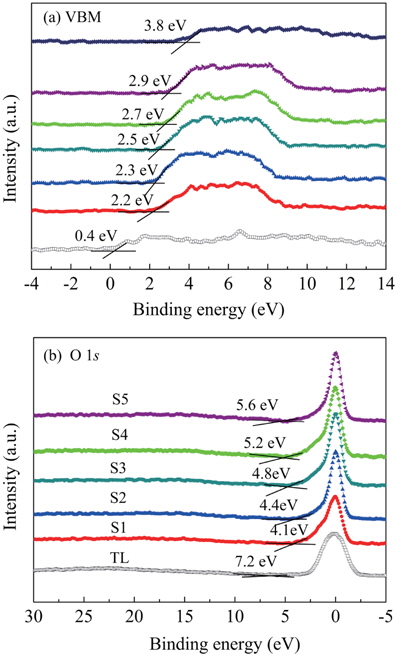
The valence band spectra and O 1s electron energy loss spectra of the five memory structures were investigated by XPS in order to understand the retention performance of the memory capacitors, as shown in Fig. 4(a) and (b). The valence band maximum (VBM) of the cleaned Si substrate is determined to be 0.4 eV by using the linear extrapolation method [16], as shown in Fig.4(a). Using the same method, the VBM at the interface of the TL/Si was determined to be 3.8 eV, and at CTL/TL for the S1, S2, S3, S4 and S5 samples, the VBMs were 2.2 eV, 2.3 eV, 2.5 eV 2.7 eV and 2.9 eV, respectively. Therefore, the valence band offset (VBO) of TL/Si was calculated as 3.4 eV by using the formula . The VBO between the TL/CTL for the S1, S2, S3, S4 and S5 are determined to be 1.6 eV, 1.5 eV, 1.3 eV, 1.1eV and 0.9 eV. The band gap (Eg) of TL and CTL are determined by the onsets of O1s electron energy loss spectra collected at the interfaces of the TL/CTL, and of the CTL/BL interface, as shown in Fig. 4(b). It is observed that the Eg of the CTL are 4.1 eV, 4.4 eV 4.8 eV, 5.2 eV and 5.6 eV for the above five memory capacitors by measuring the O1s electron energy loss spectra of CTL/BL, and the Eg of TL is determined to be 7.2 eV. Using the formula of , the calculated value of the conduction band offset (CBO) between TL/Si is 2.7 eV, where is 1.1 eV. Then the CBO between the TL/CTL are calculated to be 1.5 eV, 1.3 eV, 1.1 eV, 0.9 eV, and 0.7 eV for the five memory capacitors, respectively, and the results with respect to the energy band alignment of the memory capacitors are given in Table 1. It is worth noticing that the energy band alignments can be modulated by adding Al atoms into HfO2. As the Al content in the CTL goes up, the band gap increases gradually, whereas the CBO and VOB band offset is reduced correspondingly. It is known that the trap to band (TB) tunneling and thermal excitation (TE) are important charge loss mechanisms, which compete with each other in order to influence the data retention characteristics in the retention state [17]. At a low temperature, the TB tunneling process is the dominant charge loss mechanisms, and can be reduced by increasing the CBO, as shown in the S2 sample. S1 with maximum CBO has the worst retention performance instead, indicating that the crystallization of CTL is more crucial than a larger CBO. The TE gradually dominates the electrons loss process with an increase in temperature, and trapped electrons are thermally exited to the CTL conduction band, then tunneled back to the Si substrate. The deep energy level traps play a key role in the process. At elevated temperatures, the memory capacitors (S2, S3, S4 and S5 samples) show improved retention performance resulting from the generation of deep energy level traps by adding Al into HfO2 CTL. In order to have a quantitative understanding of the electrons loss process at high temperatures in the data retention state, we extracted the trap energy levels distribution with the change in the Al composition. At temperatures above 120℃, TE is the crucial electrons loss mechanism, and the thermal excitation constant in the CTL, eTE, are written as [18]:

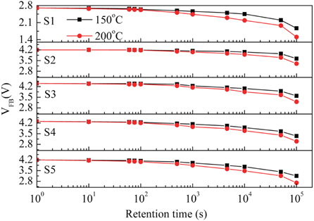
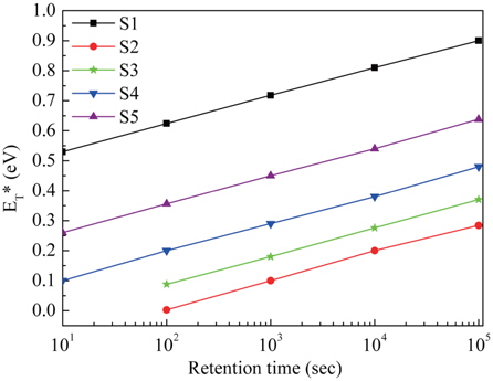
where is a combination of the temperature independent constants, , ET is the trap energy level referenced to the conduction band edge in the CTL, is Boltzmann’ constant, T is the absolute temperature (K), is the thickness of the TL (nm), q is the absolute electron charge, is the electron effective mass in the TL, is the CBO between TL/CTL (eV), and is Planck’s constant. β can be identified using the generally known physical constants. Further, α can be determined by the process described as follows. After filling all the traps with electrons and measuring the data retention characteristics of one sample at two temperatures, T1 and T2, we can obtain the times t1 and t2 when the two ΔVFB have the same value. The same ΔVFB means that the electron loss quantities in both samples have the same value because the trap density distribution does not change at T1 and T2. In our case, we measured the retention characteristics of the five memory capacitors at 150 and 200℃, as shown in Fig. 5, and α and β are listed in table 1. Hence, the maximum trap energy levels of lost charge are extracted by using the formula , as shown in Fig. 6. It is observed that can be reduced by adding Al into HfO2. In addition, the S2 sample has minimum, which results in excellent retention characteristics at high temperatures, as illustrated in Fig. 3(b). The absent data less than 100 s for S2 and S3 imply that the calculated are negative, which suggests that there are little electron loss after 100 s at 200℃ for both the S2 and S3 samples.
Charge trap flash memory capacitors incorporating (HfO2)x(Al2O3)1-x film, as the charge trapping layer, were fabricated. The effects of the charge trapping layer composition on the memory characteristics were investigated. The memory window and charge retention performance can be improved by adding Al atoms into pure HfO2, and the memory capacitor with the (HfO2)0.9(Al2O3)0.1 charge trapping layer exhibits optimized memory characteristics. The results are attributed to the large band offsets between the tunneling layer and the charge trapping layer, as identified by the valence band spectra and O 1s electron energy loss spectra. On the other hand, the (HfO2)0.9(Al2O3)0.1 charge trapping layer has minimum trap energy levels, which improve the data retention characteristics at elevated temperature. Based on this work, the charge trap flash memory device with the (HfO2)0.9(Al2O3)0.1 trap trapping layer may offer a promise as a potential candidate in future nonvolatile flash memory device applications.