통신 시스템에서 다양한 종류의 마이크로스트립 안테나는 많은 어플리케이션에서 사용되고 있다. 본 논문에서는 무선통신을 위한 2.45 ㎓의 인셋 페드 직사각형 마이크로스트립 패치 안테나를 HFSS를 활용하여 설계하였다. 안테나는 유전율 2.2, 두께 1.6 ㎜의 Telfron 기판을 사용하였으며 기판의 한쪽 면은 접지면을 갖는다. 시뮬레이션을 통하여 반사손실, VSWR, 이득, 방사패턴 등의 안테나 특성을 확인하였다.
Wireless communication has a great impact on human life since it has been developed rapidly in the past decades. In the field of wireless communications, antenna plays a vital important role. During late 1970s, there was rapid development in the field of microstrip patch antenna technology. During early 1980s, antenna elements and arrays were developed in term of design and modeling. The antenna have been largely studied due to their advantages like light weight, reduced size, low cost, conformability and the ease of integration with active device. A microstrip patch antenna is the combination of a radiating patch on one side of the dielectric substrate and ground on the other side. The patch is generally made of conducting material like gold or copper. On the dielectric substrate, the radiation patch and the feed lines are usually photo etched. Microstrip patch antennas radiate primarily because of the fringing fields between the patch edge and the ground plane. Therefore, the antenna can be fed by the various methods. These methods can be classified into two categories one is contacting and another is non-contacting. In the contacting method, the radio frequency power is directly fed to the radiating patch by using a connecting element such as microstrip line or probe feed. Whereas, in case of the non-contracting method, electromagnetic field coupling is done to transfer power between the microstrip line and the radiating patch which includes proximity feeding and aperture feeding [1, 2].
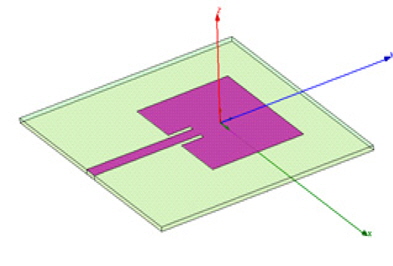
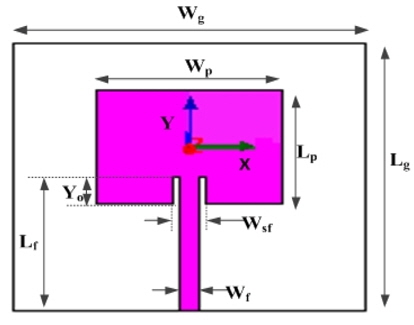
Microstrip patch antenna is characterized by a large number of physical parameters. They are designed to have many geometrical shapes and dimensions but rectangular and circular microstrip patches have been used in many applications. In this paper, the design of inset fed rectangular microstrip patch antenna at 2.45 ㎓ for wireless communication is presented having length of the patch Lp, width of the patch Wp, length of ground plane Lg, width of the ground plane Wg, inset fed distance Yo, transmission line length Lf and width Wf and Wsf is the width of the gap as shown in Figure 1. This antenna is designed on Teflon and its performance characteristic such as Return loss, VSWR, gain, radiation pattern are obtained from the simulation.
Ⅱ. Antenna Geometry and Its Design Requirement
For a rectangular patch, the length L of the patch is usually 0.3333λ0 is the free sapace wavelength. The patch is selected to be very thin such that the height of substrate h≪λ0. Thus, a rectangular patch of dimension 38.6 ㎜ × 48 ㎜ is designed on oce side of Teflon substrate of thickness 1.6 ㎜ and the ground plane of 90 ㎜ × 90 ㎜ are located on the other side of the substrate.
There are three essential parameters for design of inset fed rectangular microstrip patch antenna. They are resonant frequency (fr), dielectric material of the substrate (εr) and the thickness of substrate. The resonant frequency chosen for this design is 2.45 ㎓ .
The dielectric material of the substrate chosen for this antenna design is Teflon having a dielectric constant of the 2.2 and the loss tangent equal to 0.0009. For design purpose, the dielectric constant of the substrate material is also an important parametric factor. Low dielectric constant of the substrate material is used in the design because it gives better efficiency, higher bandwidth and the low quality factor Q. The low value of dielectric constant increases the radiated power. The designed has patch size independent of dielectric constant. So, the reduction of patch size is by using higher dielectric constant and Teflon is good in this agreement. In the simulation, the small loss tangent was neglected.
Thickness of substrate is another important in design parameter. Since thick value of substrate increases the fringing field of the patch periphery like low dielectric constant and also increases the radiated power. The dielectric substrate height of the inset fed microstrip patch antenna is h = 1.6 ㎜.
Ⅲ. Mathematical Calulation of The Antenna Parameters
The width of the antenna can be determined by
Where, λ0 =
c = velocity of light fr = resonance frequency εr = dielectric constant of substrate WP = Width of the patch
The effective dielectric constant can be determined by
Where, εreff = effective dielectric constant
εr = dielectric material of substrate h = height of dielectric substrate Wp = width of the patch
The dimensions of the patch along its length have been extended on each end by distance, the extension length is given by
The actual length L of the patch is given by
Where, fr is the resonance frequency[4]
3.3. Inset fed of the patch antenna
A physical notch is introduced by the inset feed, which in turn introduces a junction capacitance. The physical notch and its corresponding junction capacitance influence the resonance frequency. As the inset feed-point moves from the edge toward the centre of the patch the resonant input impedance decreases monotonically and reaches zero at the centre. When the value of the inset feed point approaches the centre of the patch, the where
The antenna was simulated in HFSS (High Frequency Structure Simulation) which is a high performance full-wave electromagnetic (EM) field simulator for arbitrary 3D volumetric passive device, having Microsoft windows graphical user interface. The designed antenna in HFSS simulator is shown in Figure 2.
[표 1.] 마이크로스트립 패치 안테나의 설계 파라미터
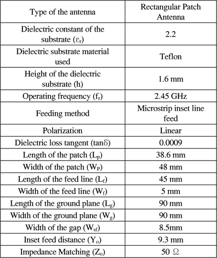
마이크로스트립 패치 안테나의 설계 파라미터
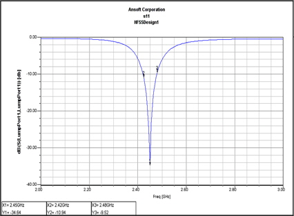
The simulation result of return loss of the inset fed antenna is -33.66 ㏈ at center frequency of 2.45 ㎓ as shown in Figure 3.
he bandwidth of the antenna in term of percentage is defined by
Where, fmax and fmin are determined at -10 ㏈. fr is the resonance frequency. The simulated value at -10 ㏈, fmax = 2.48 ㎓, fmin = 2.42 ㎓, BW = 60 ㎒ and the bandwidth percentage is 2.44%.
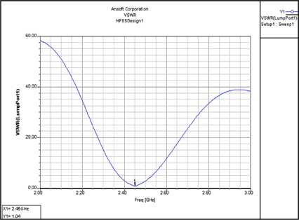
The VSWR characteristic of the antenna should falls in between 1 to 2. From simulation its value is 1.04 at 2.45 ㎓ as depicted in Figure 4.
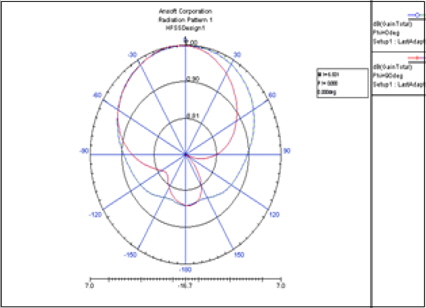
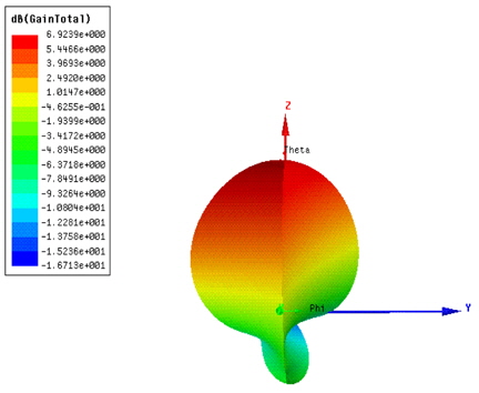
Also the radiation pattern of the antenna obtained is shown in Figure 5 at phi = 90° and phi = 0° at 2.45 ㎓. The 3D polar plot of gain is shown in Figure 6 which shows the gain of 6.9 ㏈.
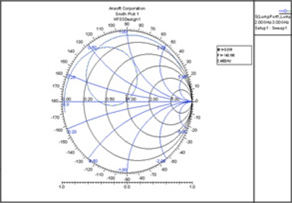
The scattering parameter for the antenna design at 2.45 ㎓ on the smith chart is shown in Figure 7.
Table 2 summarizes the obtained simulation features of the antenna from high frequency simulation software.
[표 2.] 마이크로스트립 패치 안테나의 시뮬레이션 결과
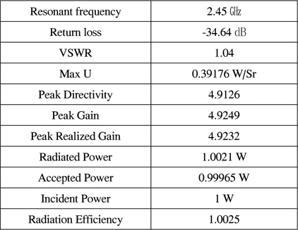
마이크로스트립 패치 안테나의 시뮬레이션 결과
In this paper, the mathematical calculation for design of inset rectangular patch antenna at 2.45 ㎓ is presented. Simulation of inset fed microstrip patch antenna is done in HFSS. The antenna performance characteristics such as return loss, VSWR, gain, radiation pattern are obtained in simulation. Hence, from simulation, the return loss obtained is -34.64 ㏈ at 2.45 ㎓; VSWR is 1.04 and gain about 6 ㏈. In future, the simulated antenna can be fabricated in PCB Board.