Multi-oxide vertical-cavity surface-emitting laser (MOXVCSEL) is expected to be a key device in cost-effective applications in the long haul and in dense wavelength division multiplex (DWDM) optical communication systems [1-4]. Recently, single mode high optical power VCSELs have been used as important sources for long haul gigabit per second data links to avoid dispersion and attenuation limitations [1]. Single mode operation in these lasers can be achieved by decreasing the radius of the active area. However, this reduction diminishes the output power due to thermal rollover limitations [3]. In fact, a solution for single mode operation of VCSELs, without improper changes in the other characteristics, is application of MOX layers [2, 3]. Due to spatial hole burning (SHB) and current crowding effects, the carrier distribution in the active layer is not uniform, which is one important reason for multimode operation of the conventional VCSELs [5, 6]. In [2] it is shown that, for a VCSEL structure with one oxide layer, there is a dip in the center and some maxima in the border of the active layer for the carrier profile. Such a carrier distribution can produce a profile suitable for multimode operation because it suffers current crowding [6]. However, by using two oxide layers, the current distribution in the active layer could be modified as a result of spreading the carrier distribution in the active layer.
The influence of different effects such as SHB, current spreading, and thermal gradients inside the cavity on the carrier distribution have been discussed by Degen et al [5]. These complex effects tend to produce higher order transverse modes in the optical cavity. The pump induced inhomogeneities control dominantly the carrier distribution [5]. These inhomogeneities arise from the current flow through the confinement area (oxide layer), not from an interaction between optical fields in the optical cavity [6]. Nakwaski and Sarzala, modeling results [7] in the distributions of current density inside the confinement region, show a maximum at the borders and a deep notch in the center of the VCSEL. They also investigated the influence of SHB on multi-mode behavior. Indeed, their results showed that the influence of SHB is much smaller than the influence of current spreading on multi-mode behavior.
The third effect that controls the multi-mode behavior refers to the strong thermal gradients in the VCSEL cavity. This effect has also been modeled by Nakwaski and Sarzala [7]. As a result of this effect, carriers are thermally re-excited and redistributed toward higher energies. This effect of spectral redistribution of carriers is stronger in the hot center of the VCSEL and is weaker in the cooler regions. Consequently, this carrier redistribution leads to a broad dip in the carrier distribution and eventually results in a multi-mode operation. However, Nakwaski and Sarzala’s results also showed that the influence of the thermal gradient is much smaller than the influence of current spreading on multi-mode behavior [7]. Moreover, electrical and thermal resistance is inversely proportional to the square of the radius of the oxide aperture. However, if the current spreads well above the aperture, it is approximately proportional to 1/r [8]. By decreasing the oxide aperture, thermal rollover occurs earlier. For a small aperture, the higher index difference suppresses the single mode operation. So, in the structures having large oxide aperture size, like those in this work, the effect of thermal gradient is much smaller in comparison with conventional structures. On the other hand, the injected VCSEL current is fixed to 10 mA in our simulations. That is much smaller than the current needed for thermal rollover.
These effects have been demonstrated by several authors, experimentally [5, 7]. The effect of inhomogeneities is dominant for governing modal behavior in the VCSEL cavity [5, 7]. Therefore, to solve the problem of multimode behavior, the profile of carrier distribution in the cavity should be improved. To overcome this problem, a two oxide layer structure was proposed [3]. By using oxide layers on both sides of the active layer and optimizing their positions and aperture sizes, the carrier distribution in the cavity could be improved. Sarzala [9] used a structure with two oxide layers as well. The top oxide aperture was wider and it was located on the anti-node position, while the second one was smaller and it was located on the node position of the optical field standing wave. The positions and thicknesses of oxide layers were fixed and their apertures were optimized to reach low threshold and single mode behavior. In [2], it was shown that by using multiple oxide layers and optimizing their positions and aperture sizes, a noticeably higher single mode output power could be achieved. The optical output power and threshold current of oxide-confined VCSEL as a function of the number, position and aperture sizes of the oxide layers were investigated. But, the thickness of the oxide layers weren’t optimized; all of them had the same thicknesses of about 80 nm.
Nobuhiko et al. [4] used an MOX structure for the purpose of widening the window aperture and maintaining single mode operation, simultaneously. Four oxide layers were used for this purpose. However, all oxide layers had the same thicknesses and aperture sizes. Neither thickness nor aperture size was optimized for having high single mode optical power.
In this paper, we use four oxide layers with the same structure proposed in [2] but the thicknesses of all oxide layers along with their positions are optimized for the purpose of the highest single mode optical output power.
In Sect. 2, the VCSEL structure is presented briefly, based on the structure proposed in [2]. Then, the model of the VCSEL under consideration is presented. Numerical results of the oxide layer thicknesses and positions on VCSEL performance are discussed in Sect. 4. Finally, the paper is concluded in Sec. 5.
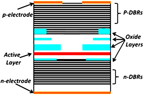
II. THE STRUCTURE OF THE MOX VCSEL
For comparing the structure with different oxide layer thicknesses and the structure with the same oxide layer thicknesses, the MOX VCSEL structure under consideration is selected as proposed in [2]. The only difference is the thicknesses of oxide layers and their positions, which are optimized here to reach the highest single mode output power. The structure of VCSEL under consideration is shown in Fig. 1. As is clear from the figure, the structure has four oxide layers located on the optimized positions and has the optimized aperture sizes and thicknesses. One oxide layer is located at the bottom and three oxide layers are located on the top of the active layer. To avoid the complexity of the optimization procedure, the number of oxide layers and their aperture sizes are selected from the reported results of [2].
Oxide layer thickness is another parameter that could be optimized, giving another degree of freedom for VCSEL design. But, the oxide thickness variations can cause the effective index difference Δneff to be changed. So, the single mode operation may be suspended. To have a constant Δneff, the oxide layer position and thickness must be changed simultaneously.
Here, the four oxide layer thicknesses and their corresponding positions are optimized concurrently to have maximum single-mode optical output power. For more details of the structure one can refer to [2]. In this paper, the four oxide layer thicknesses and their corresponding positions are optimized concurrently to have maximum single-mode optical output power. For more details of the structure one can refer to [2].
The intense interaction of optical, electrical, and thermal phenomena occurring in the VCSEL operation, their effects must be taken into account in the VCSEL model. Recently, various methods have been introduced to improve the accuracy of optical solution [10]. In this paper, a VCSEL simulator which applies a vectorial three-dimensional selfconsistent electro-thermo-optical model is used. Although the vectorial models are accurate, the complexity of these methods makes the self-consistent electro-thermo-optical simulation impractical with regard to the calculation time. For VCSEL simulation, the vectorial models are reduced to the scalar forms to get a reasonable calculation time.
The computer model used to simulate room-temperature operation of the VCSEL consists of four principal parts:
A. Optical Model: Successive optical modes and the electromagnetic field within the laser resonator are described by the optical model. Maxwell vectorial equations are reduced to the scalar Helmholtz equation in cylindrical coordinates. A well-developed effective index model is used to solve the Helmholtz equation [11, 12]. This method is often referred to as the Effective Frequency Method (EFM), which is a fast and flexible method in analysis of VCSELs [10, 11].B. Electrical Model: The electrical model characterizes both the current spreading (including carrier diffusion) between the top and bottom contacts and the injection of carriers of both kinds into the active region. The Poisson equation is solved by using the finite element method (FEM). Finally, by using the Laplace equation, current densities in VCSEL can be calculated [12]. By solving these equations and the Poisson equation (by a finite element method, for example) in the active region, current spreading and carrier densities within the active region are calculated [13].C. Thermal Model: The thermal model characterizes generation of a heat flux (irradiative recombination, re-absorption of spontaneous emission as well as volume and barrier Joule heating) and its spreading from heat sources towards heat sinks. The finite element method is used for solving thermal equations. The heat equation below is solved by using the FEM [12].
Where T is the spatial variation of the temperature distribution, κT is the material thermal conductivity, and ρT is the distribution of internal heat source density. D. Gain Model: The standard gain model is applied to calculate optical gain [14-16].
In addition, the VCSEL model has a self-consistent part which describes all interactions between the above physical effects. In other words, electrical equations, Helmholtz equation, thermal equation and the gain equation are solved self-consistently. The non-linear solution and the iteration method and their parameters, such as convergence criteria and iteration number, are specified in the model to converge the solution. The system of nonlinear equations that result from FEM on a mesh are solved iteratively starting from an initial value [16]. Results obtained from solving the linearized problems provide corrections that are used to update the ongoing estimation of the solution. Iteration continues until convergence criteria are met and in this case, the solution will be accepted. If the iteration number passes a maximum allowable number, a different technique is tried. In this case, a different grid, a different initial value, or a different non-linear iteration technique is tried. For more details of the mathematical model one can refer to [2].
IV. NUMERICAL RESULTS AND DISCUSSION
4.1. Oxide Layer Thickness Effects
Oxide-confined VCSELs are very sensitive to the characteristics of oxide layers [2, 3]. In fact, small changes in oxide layer position, aperture size or thicknesses, cause notable variations on the VCSEL performances such as output power, threshold current, number of modes, modulation speed, etc. So, the optimization parameters (such as thickness, location, and aperture size of each oxide layer) increase noticeably by increasing the number of oxide layers, causing the optimizing procedure to become a hard task. An optimizing procedure was suggested in [2] to optimize the number of oxide layers and the aperture size and location of each oxide layer. The optimization process for optimizing the number of oxide layers and aperture size and location of each oxide layer were discussed in detail in [2]. However, the thicknesses of all oxide layers were kept fixed to 80 nm for the purpose of modulation speed maximization. In this paper, the number, and aperture size of each oxide layer is selected using the results of [1]. The thickness of oxide layers is optimized to reach the highest single mode optical output power. The optimizing process is still cumbersome since the thicknesses of four oxide layers aren’t independent and should be optimized simultaneously. If the parameters were independent of each other, the thickness of each oxide layer could be optimized separately. However, changing the parameters of one oxide layer affects the parameters of other oxide layers causing the optimizing process to be cumbersome. On the other hand, changing the oxide layer thickness changes the optimized location of oxide layers.
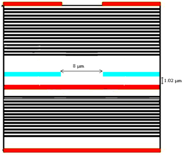
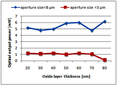
To obtain some insight by using different oxide layer thicknesses, it is useful to consider the influence of one oxide layer thickness on VCSEL performance. For this purpose, we use a conventional oxide-confined VCSEL having one oxide layer by 8 μm aperture size. This structure is plotted in Fig. 2. One important effect of oxide layer thickness is the modulation speed decrement [4]. In fact, the thin oxide layer causes high parasitic capacitance. So, conventional oxide-confined VCSELs suffer from limited modulation speed. Therefore, it is useful to increase the total thickness of the oxide layer to achieve a low parasitic capacitance, consequently achieving a higher modulation speed. So, the MOX structure can be used for high modulation speed applications. Increasing oxide layer thickness increases Δn, the cavity index difference, too. Therefore, the confinement factor is increased and as a result, the number of modes will be raised. A higher threshold gain, gth, is needed so that threshold current and scattering loss are increased [5]. For big aperture size VCSELs, the oxide thickness does not have a significant influence on gth and optical scattering loss [5]. For a given oxide thickness, if the oxide layer approaches the active region, Δn increases [5]. Decreasing the oxide position with a given thickness increases Δn as well. Δn could be kept constant by increasing both thickness and the distance from the active region. This feature facilitates the optimization procedure. Inordinate decrease of oxide thickness causes the oxidation rate to depend on the oxide thickness. As a result, the oxidation process will be more complicated [5]. To show the influence of oxide layer thickness on optical output power, the oxide thickness of the structure, shown in Fig. 2, is changed from 10 to 90 nm. The result is plotted in Fig. 3. Note that the optical output power of the 8 μm aperture size is multi-mode. Single mode operation for one oxide layer structure can only be achieved for apertures as small as 3 μm [2, 3]. So, for comparison, the results for the structure containing 3 μm aperture sizes are shown in Fig. 3. It should be pointed out that, by changing the oxide layer thickness the single mode operation for 3 μm aperture size structure might be stopped. So, the oxide position for this structure is changed as well retaining the single mode operation.
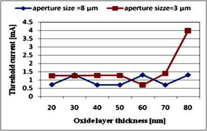
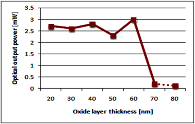
To study the influence of oxide layer thickness on single mode behavior, the oxide layer is located at 1.02 μm. In Fig. 4, the optical output power of a structure with 3 μm aperture size is plotted as a function of oxide layer thickness. As it is clear from Fig. 4, there is only a single mode operation for thicknesses more than 70 nm plotted by dotted line. Threshold currents as a function of oxide thicknesses are plotted in Fig. 5. As is clear from the figure, for 8 μm aperture size, threshold current changes slightly but for 3 μm aperture size; its variations are remarkable. This is due to the higher scattering losses for small aperture VCSELs which are more sensitive to oxide layer thickness. So, for smaller aperture size and thick oxide layers, threshold current is much higher than for the big aperture size, and it is in agreement with the results of [11].
[FIG. 5.] Threshold current as a function of oxide layer thickness for two different aperture sizes.

So, the oxide layer thickness has considerable influence on VCSEL performance, giving another degree of freedom for VCSEL design.
4.2. Optimizing the Thicknesses of Oxide Layers
As described in the previous section, multiple oxide layers with different thicknesses and aperture sizes in the VCSEL structure were used to control the current distribution. By varying the number of oxide layers and using an optimizing process, it is possible to reach a desirable structure with optimized output power in single mode operation. In fact, by relative displacement of the oxide layer positions, relative aperture sizes, and oxide layer thicknesses, the spatial carrier distribution can be optimized. Higher aperture sizes also have an important impact on the thermal behavior [16]. So this structure is expected to have high optical output power, low threshold current, high speed modulation and better thermal behavior. Since there are many parameters, optimizing all of them is extremely cumbersome. For optimizing this structure, we use the results of our previous work [2]. The number of oxide layers, and the aperture size of each oxide layer were optimized to achieve the highest single mode output power.
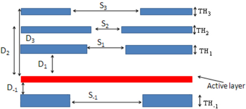
To compare the optical output power of all VCSEL structures, the injected VCSEL current is fixed at 10 mA for different structures. To show the optimizing procedure, the details of oxide layers are addressed by Si, Di, and THi as shown in Fig. 6. In this figure, Si, Di and THi are the size, location, and thickness of the i-th layer, respectively.
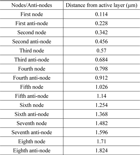
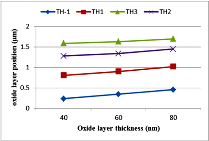
To optimize thickness of oxide layers, all oxide layers must be changed simultaneously. This is because the oxide layer details aren’t independent. So, TH-1, TH1, TH2, and TH3 are changed from 40 to 80 nm and for each state, the position of each oxide layer is changed to achieve the maximum single mode optical output power. As the cavity index difference could be kept constant, by decreasing or increasing both thickness and position of oxide layer, the optimizing procedure for finding the position of oxide layers is simpler. For each oxide layer thickness, the oxide layer position of each oxide layer is changed from one node (or anti-node) to another adjacent node (or anti-node) of optical standing wave to keep single mode operation. Table 1 presents the node and anti-node of optical standing wave location in both sides of the active layer.
[TABLE 1.] Node and anti-node of optical standing wave

Node and anti-node of optical standing wave
For example, consider the case in which THi are all 40 nm. For this structure, all oxide layer positions are decreased from the previous optimized position to another node of optical standing wave to reach the single mode operation. For each oxide layer, the oxide layer thickness is changed from 40 to 80 nm and for each state the position of each oxide layer is changed to reach the single mode operation. The results of the optimized position of each oxide layer as a function of oxide layer thickness are shown in Fig. 7.
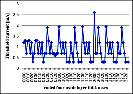
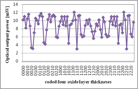
So, there are four variables (four oxide layer thickness) that must be changed. In fact, the optical output power depends on four variables and hence, plotting the diagram of the optimized results is impossible. To overcome this problem, a properly coded scheme is proposed for four variables. In this method, 40, 60, and 80 nm oxide layer thicknesses are corresponding to 0, 1, and 2 respectively. For instance, 0000 means that all oxide layers are equal to 40 nm, and 1021 means that TH-1, TH1, TH2, and TH3 are equal to 60, 40, 80, and 60 nm, respectively. The optical output power as a function of coded oxide layers is plotted in Fig. 8.
As it is clear from Fig. 8, by changing the oxide layer thicknesses, the optical output power is changed noticeably. The highest optical output power of 12 mW is achieved by optimizing the oxide layer thicknesses. To find the threshold current, the optical output power for another lower current is calculated and the threshold current is determined, considering a linear L-I curve. The threshold current of proposed MOX structure as a function of coded oxide layers is plotted in Fig. 9.
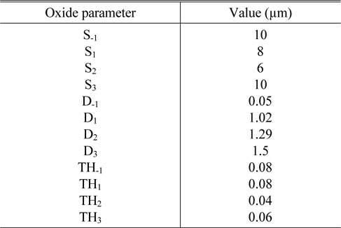
As seen, the maximized optical power occurs at two points; one at 1101 and another at 2201. The corresponding threshold current is 0.7 mA for both cases. However, the second point (2201) is more desirable for high speed modulation purposes. This is because this structure has thicker oxide layers. Table 2 presents the details of optimized oxide layers.
[TABLE 2.] Optimized results of MOX VCSEL structures

Optimized results of MOX VCSEL structures
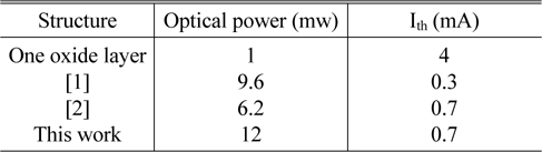
The final optimized structure generates an optical output power in single mode operation of about 12 mW. This structure has 25% more optical power as compared to the MOX VCSEL with the same oxide layer (with thicknesses equal to 80 nm corresponding to 2222 coded case). The corresponding threshold current of this structure is 0.7 mA which is comparable with the previously mentioned structure. This structure, compared to the previous structure, still has a simple design and thus low manufacturing cost. The comparison of different structures is summarized in Table 3.
[TABLE 3.] comparison of different VCSEL structures

comparison of different VCSEL structures
In this paper, by using multiple oxide layers in the VCSEL structure with different aperture sizes and oxide thicknesses, the output optical power in single mode operation is maximized. The optical output power is plotted as a function of four oxide layers’ thicknesses using a proposed coding method. The proposed MOX VCSEL has 12 mW single mode optical output power and 0.7 mA threshold current. The proposed MOX VCSEL is extremely desirable for high speed high power applications. For one oxide layer, the maximum optical power and threshold current were 1 mW and 4 mA, respectively. The proposed structure is compared with other structures showing higher optical power and comparable threshold current. The oxide layer thickness gives another degree of freedom for designing VCSELs. Using multiple oxide layers offers a very useful technique for single mode high power VCSELs without higher complexity in either growth or processing. Also, this structure has higher speed modulation when compared with conventional oxide-confined VCSELs as a result of bigger total oxide layer thickness.