ZnO is a semiconductor with direct band structure (band gap energy of 3.37 eV at room temperature), which is similar in physical characteristics to GaN. Carrier doping is the first barrier to be overcome for the application of ZnO as electronic and photonic devices. While n-type doping can be easily realized to the level up to 1021 cm-3 [1], reports on successful p-type doping are rare but gradually increasing [2, 3]. Both bipolar (n-and p-type) doping and wide band gap could maximize the possibility of developing ZnO as transparent electronic devices and light emitting devices from visible to uv regions[4-7]. In addition, the high exciton binding energy of ZnO (~60 meV, cf. ~25 meV for GaN) allows near-band-edge excitonic emission at room and higher temperatures [5, 6, 8, 9]. Recently, the technology enabling us to exploit ZnO is developing fast, however, the fundamental understanding for optical characteristics is still under debate. Besides such a physical understanding, various physical and chemical treatment processes should be linked in order to realize promising devices of ZnO.
Photoluminescence (PL) investigation is a suitable tool to determine the crystal quality and the presence of impurities in the material. In addition, the study at low temperatures gives more detailed comprehension of the physical properties of the sample. In this article, we studied the effects of O-plasma treatment on the physical characteristics of ZnO thin films with PL spectroscopy, varying sample temperatures from 10 K to 290 K.
The sample used in this experiment was ZnO thin films of thickness ~350 nm grown on c-plane sapphire at 650℃ by rf-magnetron sputtering in an Ar+O2 ambient atmosphere. After chemical cleaning, the sample was showered at 300℃ in O-plasma generated by an RF plasma system. The experimental conditions for the plasma treatment are shown in the Table 1. PL measurement was performed as the sample was kept in the closed cycle cryostat. The sample temperature was varied from 10 K to 290 K. The excitation source was a CW He-Cd laser (λ=325 nm).
[TABLE 1.] Experimental conditions for the O-plasma treatment
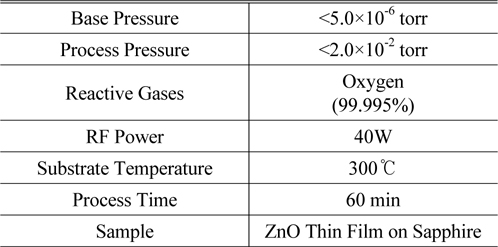
Experimental conditions for the O-plasma treatment
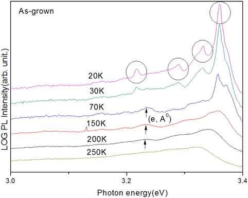
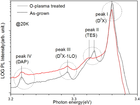
The experimental results of this work are based on the analysis of PL spectra from ZnO thin films. The spectra were taken at the varying temperatures of the sample from 10 K to 290 K from two differently prepared samples, one of which is “as grown” and the other is “O-plasma treated”. There was spectral similarity between the two samples, as shown in Fig. 1, where four characteristic peaks (Peak I, II, III and IV) were identified for each sample. Now the physical origins for each peak and the resulting effects of O-plasma treatment on ZnO films will be examined.
In the undoped bulk ZnO, the neutral shallow donor bound exciton often dominates because of the presence of donors resulting from unintentional impurities and/or shallow donor-like defects [10]. Acceptors like Na or Li could be present in ZnO, too [11]. However, the chemical origin and binding energy of the most underlying donor and acceptor atoms remain unclear. It is known that the low-temperature PL spectra are dominated by several bound excitons in the narrow energy range from 3.348 to 3.374 eV[12]. The higher energy part of the range is mainly due to the recombination of neutral donor-bound excitons (D0X), while the lower part comes from neutral acceptor bound excitons (A0X) [12]. Peak I in Fig. 1, appearing at 3.360 eV for both samples (as grown and O-plasma treated), is believed to be mainly the recombination of D0X, which is in good agreement with the results reported by other groups [12-15].
When D0X decays, all the energy of the exciton is converted into the energy of a photon. However, the decay process could involve TES (Two Electron Satellites) transition, where the donor atom is excited to a higher energy state. When this happens, the outcoming photon will have less energy by an amount equal to the energy difference between the first excited and ground states of the donor. For ZnO, the difference is known to be around 30 meV, which varies with the donor atoms that localize D0X [12, 13, 16]. The TES transition could be identified in our study. Peak II of our spectra depicted in Fig. 1 is considered to be related to the TES transition. Unlike Peak I (D0X), however, Peak II appears at different positions according to the sample preparation. The positions are as follows: 28 meV lower than Peak I for as-grown samples and 35 meV for O-plasma treated samples. What this observation implies will be discussed later.
Peak III, appearing at 3.289 eV at 20 K, whose energy is lower than Peak I by about 71 meV, is believed to be due to a phonon replica of Peak I, as the longitudinal optical (LO) phonon energy of ZnO is known to be 71-73 meV [17].
When there exists both donor and acceptor impurities together, the recombination of an electron and a hole can take place via donor-acceptor pair (DAP) transitions. The DAP transition, which is observed at low temperatures, happens through a quantum tunneling process when impurities are further away from each other than effective Bohr radius. The photon energy for the DAP transition is as follows; hν = Eg - ED - EA + q2/ϵr [18]. The experimental evidence for the DAP transition is found in many other works, and the outgoing photon energy related to the DAP transition is known to be near 3.22 eV for ZnO [12, 16, 19, 20]. The DAP transition could be identified in our experiment, too. Peak IV, appearing at 3.217 eV for both samples, is considered to be the emission from the DAP transitions.
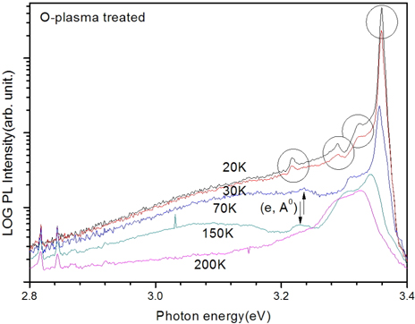
Figure 2 and Fig. 3 show the evolution of PL spectra with sample temperatures for O-plasma treated and as-grown samples, respectively. Common features can be found in the both figures. The Peak III and IV, which are distinct in spectra at low temperatures of 10 K-30 K, become obscured at higher temperatures. This, instead, accompanies the generation of a new peak positioned at 3.23-3.24 eV which is designated by an arrow in the figures. The new peak was distinguishable up to 200 K for as-grown samples and 180 K for O-plasma treated samples. This experimental observation indicates the thermal ionization of neutral donors. Donors in ZnO get thermally ionized more and more as the temperature gets higher. Free electrons from the neutral donors are expected to recombine with the neutral acceptors, which is denoted by the free electron-acceptor transition (e, A0). This (e, A0) peak will appear at higher energies than the DAP peak, and similar results were reported in other works [12, 16, 19]. Hence, the newly-rising peak at 3.23-3.24 eV is believed to be the emission from the (e, A0) transition.
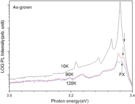
Figure 4 shows spectral evolution with temperatures for the as-grown sample, where a new peak, designated by arrows, could be identified at the right shoulder of Peak I (D0X). The peak gets more distinct as temperature increases. The position of the peak is 3.369 eV at 90 K, which is higher by 14.1 meV than the D0X peak. We believe that this peak comes from the decay of the free exciton, considering the relative position of the peak to D0X along with characteristic features of temperature evolution. The localization energy of bound excitons in ZnO is known to be 10-20 meV[12, 14, 15, 20], which is in a good agreement with our result. This indicates that bound excitons change into free excitons as the temperature increases. The free exciton peak gets larger with the increase of the temperature, and starts to surpass the D0X peak at 120 K, as shown in the figure. This tendency continues, and free excitons are dominant from 150 K.
Let us consider the effects of O-plasma treatment on the properties of ZnO film. The plasma treatment process can induce both physical and chemical effects on the sample. The atoms and/or ions in the plasma will penetrate into the sample, damaging the crystal and making chemical bonds with the atoms in the sample. As a result, the plasma process induces crystal defects as well as impurities in the sample. Oxygen atoms and ions in the O-plasma are expected to make chemical bonds with donor-like impurities and defects which are known to exist in an undoped ZnO. They can also fill O-vacancies which are known to play an important role as donors in ZnO along with interstitial Zn atoms. As a result, the density of the donor-like defects decreases in the plasma process, which results in decrease of the intensity of D0X and DAP transitions. This was identified in our experimental result. Comparing the intensities of the D0X peak and the DAP peak for both samples at 10 K, we could find that the intensity decreased by about 40% for the D0X peak and 60% for the DAP peak after the plasma treatment. Oxygen atoms and defects, which are generated in the sample during the plasma process, can become new centers that localize excitons. Some of those centers will act as neutral donors to capture excitons, which results in another D0X. The difference in the position of Peak II between both samples, as stated above in Fig. 1, can be understood to be due to newly generated neutral donors after the O-plasma treatment.
Another feature, to be noted, is that the remarkable recombination of free excitons was not identified for the O-plasma treated sample. It is difficult to determine the physical origin of the phenomena based solely on our data, but it is suggestive that the higher defect and impurity concentrations induced in the sample by O-plasma can make the formation of free excitons difficult and the lifetime of the free exciton shorter. Hence, the peak from free excitons seems to be shaded after the plasma treatment.
The PL intensity concerning DoX and DAP decreased after the O-plasma treatment by 40% and 60% respectively at 10 K. These two emissions are closely related to neutral donors in ZnO, which indicates that the O-plasma process induces a remarkable decrease of neutral donors. Considering that the O-vacancies and interstitial Zn atoms play an important role as donors in ZnO, the result implies that oxygen atoms and ions in the O-plasma penetrate into the film, filling O-vacancies and making chemical bonds with interstitial Zn atoms. And crystal defects and impurities caused during the O-plasma process are expected to become new centers that localize excitons, which is responsible for the different position of TES emissions (28 meV lower than DoX for as-grown samples and 35 meV for O-plasma treated samples). In our study, no significant trace of free excitons has been observed in the PL data after the O-plasma treatment. This could be attributed to higher defect and impurity concentrations generated in the sample by the O-plasma treatment.