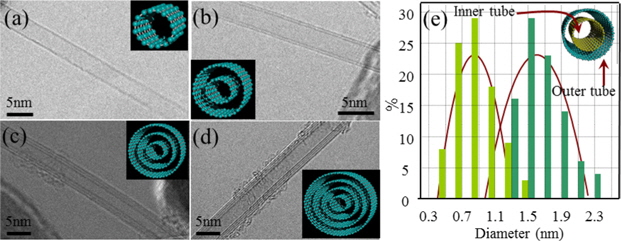
Tiny one-dimensional carbon nanotubes with nanoscale dimensions have attracted a great deal of attention, not only from a fundamental scientific point of view but also from a technological standpoint [1-8]. Their unique structures afford interesting physical and chemical properties, and these excellent properties can potentially be exploited in fabricating diverse industrial products. Carbon nanotubes, considered as pure polymer chains of carbon, are seamless cylindrical forms with nanometer size, consisting of single or concentric multilayers of graphene sheets (single walled carbon nanotubes (SWCNTs) or multi-walled CNTs [MWCNTs]) (Figs. 1a-d). In recent years, double walled CNTs (DWCNTs) have attracted the attention of numerous scientists because their intrinsic coaxial structures (Fig. 1b) give rise to intriguing electronic and mechanical properties that have not been reported hitherto. By judiciously preparing high-purity DWCNTs we were able to examine whether they behave as quantum wires and whether there is a chirality relationship between concentric tubes during growth. We also assessed the shell effect on the concentricity on the electronic conductance and the adsorption properties of a coaxial nanotube rope. When compared to SWCNTs and MWCNTs, DWCNTs are considered preferred materials for field emission display sources, nanocomposites, nanotube bi-cables, electrochemical electrodes, hydrogen storage materials, atomic force microscopy tips, and various electronic devices. Within these contexts, intensive studies on the synthesis, characterization, and possible application of DWCNTs have been carried out during the past decade. In this article, we review the synthesis techniques of DWCNTs, their interesting electronic and transport properties, and promising applications.
2. Synthesis of Catalytically Grown High Purity DWCNTs
The DWCNTs were catalytically grown by the chemical vapor deposition (CVD) method utilizing an iron-based catalyst. Methane was fed into the reactor typically for 10 min at 875℃ [9,10]. The optimized reaction temperature for obtaining high-purity DWCNTs was 875℃, when using methane as the carbon feedstock and iron as the tube catalyst. An important factor affecting the preferential growth of DWCNTs over MWCNTs is maintaining the size of the metal particles below 3 nm and the most critical factor for the selective growth of DWCNTs over SWCNTs is increasing the amount of active carbon species. Metal particles containing a higher amount of dissolved carbon will be more favorable for the formation of DWCNTs over SWCNTs. From this argument, it is expected that the inner shell and outer shell grow simultaneously.
In order to obtain high quality DWCNTs, a purification process was applied to synthesize these products. First, an oxidation process (500℃, 20 min) was carried out to reduce the amount of chemically active SWCNTs. Second, hydrochloric acid (18%, 100℃, 10 h) treatment was carried out to remove magnesium oxide and iron catalysts, followed by air oxidation at 500℃ for 10 min to remove carbonaceous impurities. A detailed high resolution transmission electron microscopy (HR-TEM) analysis confirmed the high yield of DWCNTs (above 95%) in bundles with relatively homogeneous and small-sized inner tubes of mainly ca. 0.9 nm diameter and outer diameters of ca. 1.5 nm (see diameter distribution of DWCNTs in Fig. 1e). Magnetic susceptibility studies confirmed the high DWCNT sample purity through their diamagnetic behavior.
3. Fabrication of Thin, Flexible, and Tough DWCNT Buckypaper
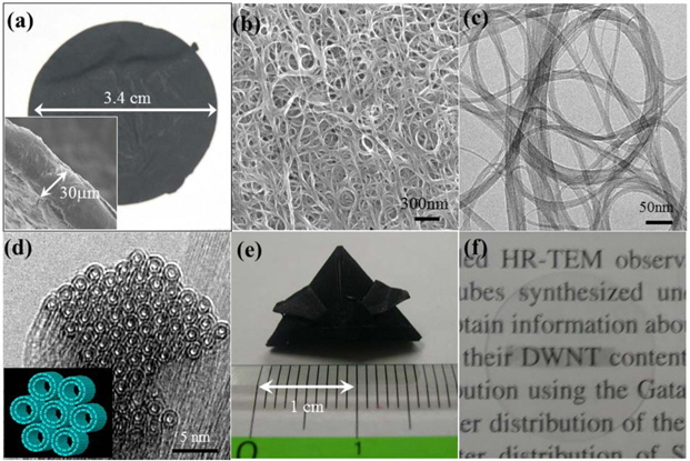
Nano-sized carbon nanotubes have a high tendency toward self-aggregation due to strong Van der Waals forces [11]. By utilizing this intrinsic property, it is possible to obtain paperlike sheets from carbon nanotubes dispersed in solution [12]. First, a stable suspension of DWCNTs should be prepared with the help of ultra-sonication. By very carefully pouring the stable suspension of nanotubes into a polytetrafluoroethylene filterattached funnel, very thin (ca. 30 μm), round (diameter = 3.4 cm), light (weight = ca. 15 mg) and black buckypaper can then be produced (Fig. 2a). As expected, buckypaper is the result of physical entanglement of DWCNT bundles (10-30 nm) (Fig. 2b). From the cross-sectional HR-TEM image (Fig. 2d), DWCNTs consist of two relatively round, small and homogeneoussized (below 2 nm at the outer shell) concentric individual tubules. Furthermore, these co-axial tubes are packed in a hexagonal array. This DWCNT buckypaper is highly flexible and is mechanically strong enough to fold into origami (Fig. 2e). The high structural integrity of DWCNT-derived buckypaper is thought to be derived mainly from the significant lengths of the tubes, because the longer the tubes are, the greater is the mechanical robustness of the intermingled bundles. It should be noted that we fabricated rectangular semi-transparent films on a round glass cover by utilizing a very small amount of DWCNTs (the acronym “DWCNT” is clearly seen in Fig. 2f).
4. Raman and X-ray Diffraction Characterizations
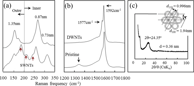
The diameter distribution and the structural perfection of the materials were evaluated using Raman and X-ray diffraction (XRD) studies. Fig. 3 shows Raman spectra in the low frequency (radial breathing mode, RBM) and high frequency (tangential G-band mode) ranges, respectively. The low frequency Raman spectra confirm the disappearance of RBMs assigned to SWCNTs (see short arrows around 180, 210, and 240 cm−1 in Fig. 3a) after purification, indicating the effective removal of chemically active SWCNTs. In addition, we confirmed the effective removal of deposited carbon on the outer surface of the carbon nanotubes from the largely reduced intensity of the D-band (defect-induced, double-resonance Raman scattering feature [13]), as shown in Fig. 3b. It is noteworthy that the D-band for DWCNTs is negligible in the Raman spectra. We also noticed relatively well-developed (100) and (110) diffraction lines from XRD measurements of the DWCNTs, thus indicating that the tubes are highly crystalline. It is also observed that the average interlayer spacing is 0.36 nm, which is substantially larger than that of MWCNTs (ca. 0.339 nm) (Fig. 3c). It is well known that the RBM frequency inversely depends on the tube diameter [14]. For DWCNTs, the Raman RBM features above 250 cm−1 correspond to the inner tubes, whereas peaks below 250 cm−1 are associated with the outer tubular shells. The dt values in Fig. 3a indicate the tube diameters calculated using the equation
5. Thermal Stability of DWCNTs
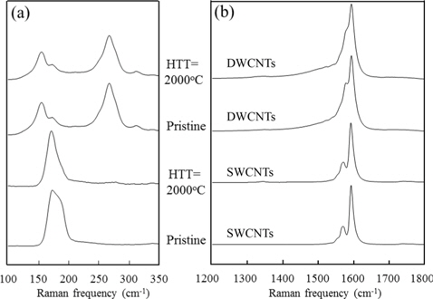
It is expected that the coaxial structure of DWCNTs lends them good stability during thermal treatment under an argon atmosphere, because a structural transformation was first observed at ca. 800℃ for nanohorns and at ca. 1200℃ for a catalytically grown SWCNTs [16]. For a comparative study of the thermal stability of DWCNTs, arc discharge-derived highly purity SWCNTs was used because these SWCNTs are believed to exhibit high structural integrity due to their high synthesis temperature (above 1500℃). Both samples were thermally treated at 2000℃ for 30 min using a graphite-resistance furnace. As shown in Fig. 4, we could not identify any changes in the Raman spectra for the DWCNTs thermally treated at 2000℃. On the other hand, reduced width of the RBM and a slightly intensified D-band were observed after thermal treatment of SWCNTs (Fig. 4). For thermally treated SWCNTs, two- or three-fold increased bundle size of SWCNTs was confirmed. From cross-sectional TEM images of SWCNTs, a large portion of round and small-sized (ca. 1.4 nm) SWCNTs in a single SWCNT bundle were structurally transformed into distorted and large-sized (ca. 4-5 nm) tubes via the well-known merging process [17]. Therefore, the Raman signals from the thermally treated SWCNTs (Fig. 4) are resonance resulting from the remaining SWCNTs. The appearance of the shoulder peak at 180 cm-1 and the D band for thermally treated SWCNT bundles thus indirectly indicates the structural transformation from less stable small-sized tubes to more stable large-sized tubes through a zipping mechanism [17]. On the other hand, there was no structural change in the case of DWCNTs thermally treated at 2000℃.
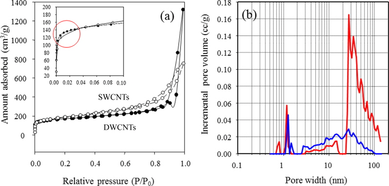
6. Pore Structure and Oxidative Stability of the Bundled DWCNTs
This section describes the surface properties of DWCNT buckypaper, including its oxidation stability compared with that of SWCNTs [14], with the aim of understanding the structural differences between bundles of single graphene tubules and DWCNTs ropes. Fig. 5a shows the N2 adsorption isotherms for SWCNT- and DWCNT-derived buckypaper, respectively. DWCNTs exhibited a steady uptake of N2 at a medium relative pressure (P/P0) and an abrupt uptake of N2 at high relative pressure (above 0.9), similar to a typical type II isotherm, whereas the adsorption isotherms for SWCNT-derived buckypaper show a hysteresis loop at high relative pressure, corresponding to a typical type IV isotherm. An abrupt increase in the N2 uptake below
Also, the resistance to oxidation was compared for both tubes using a thermal gravimetric analysis in an argon and oxygen (1%) gas mixture (Fig. 6). By taking the first derivative of Fig. 6, the temperature at which the rate of combustion is highest is obtained. The results demonstrate that the DWCNTs are oxidized at a significantly higher temperature (ca. 717℃) when compared to the SWCNTs (ca. 541℃). It is believed that the high resistance to oxidation of the DWCNTs is derived from their structural features (namely the “coaxial structure”) as well as the high crystallinity of the bundles. It is very interesting that the DWCNTs are also structurally stable when they are thermally treated up to 2000℃, whereas SWCNTs are known to show structural corruption at 1300℃.
Since the discovery of band gap photoluminescence (PL) from isolated SWCNTs [18,19], PL maps have been widely utilized for determining the relative (
It has been reported that the inner tubes of CVD-grown DWCNTs with small diameter are preferred over SWCNTs for producing photo-luminescent materials [26,27]. Due to their coaxial structure, the inner tubes of DWCNTs are expected to possess higher structural perfection and to be more resistant towards environmental changes when compared to SWCNTs. Strong and environmentally stable PL was seen from the inner tubes of the DWCNTs (Figs. 7a and b) as compared to SWCNTs. This was ascribed to possible energy transfer from the outer tubes to the inner tubes, especially for smaller diameter tubes, and the protective effect of the outer tubes during the purification and dispersing processes. However, in order to elucidate the intrinsic optical features of the inner tubes within DWCNTs, the quantum efficiency and extinction coefficient for the inner tube of an individual DWCNT should be measured and compared with the corresponding results previously reported for SWCNTs. Furthermore, the energy transfer mechanism between the inner and outer tubes should be elucidated.
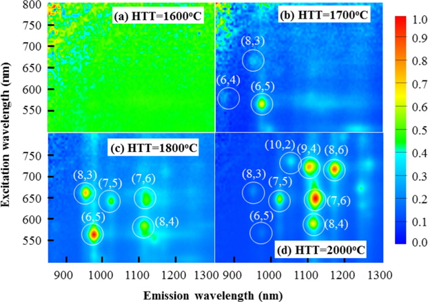
In addition, bright PL signals from the inner tubes of DWCNTs (Fig. 8) prepared by thermally treating peapods at high temperatures of 1700-2000°C in argon were reported [28]. It was suggested that the fraction of metallic corrugated tubes in the inner tubes of the DWCNTs act as energy drains that quench the PL signals. At a specific temperature, the metallic corrugation of the inner tubes of DWCNTs is reconstructed to form a well-defined semiconducting (more energetically stable) tube, and the PL signals start to appear again.
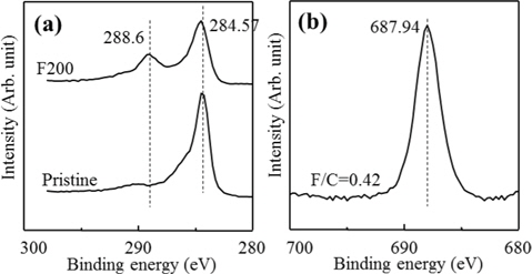
This section describes the preparation of fluorinated DWCNTs by directly reacting elemental fluorine at 200℃ [29,30]. One of the structural advantages of DWCNTs over SWCNTs is that fluorine atoms can be selectively attached to the outer shell of DWCNTs, leaving the inner shell of the DWCNTs intact.
Fig. 9a shows the
According to a low-resolution TEM study (Fig. 10a), the DWCNTs in this study exist mainly in a bundled state, and the sizes of DWCNT bundles are in a range of 10-50 nm. In addition, typical cross-sectional HR-TEM images of DWCNTs show that they are hexagonally packed in bundles (Fig. 10b). No distinctive changes in the macro-morphology of DWCNTs are found through fluorination (Fig. 10c). It is noteworthy that double-layered cylindrical shells are clearly seen (Fig. 10d) in high resolution cross-sectional images of the fluorinated DWCNTs. Furthermore, the hexagonal packing structure of the bundles is disturbed, possibly due to chemically incorporated fluorine atoms on the outer shells of the DWCNTs.
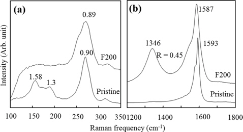
Low frequency Raman spectra for the pristine and fluorinated DWCNTs (Fig. 11a) were measured in order to determine the RBM frequency, which is inversely related to the tube diameter. Raman lines appear above 250 cm−1 (corresponding to the inner shells of the DWCNTs), and below 250 cm−1 (associated with the outer shells of the DWCNTs). Even though there was no significant change in the frequencies for the peaks at ca. 270 and 324 cm−1 corresponding to the inner shells, the RBM frequencies originating from the outer shells of the DWCNTs are clearly depressed through fluorination. It is noted that the double-layered morphology of the fluorinated DWCNTs is clearly seen by the crosssectional HR-TEM observations. The depression of the RBM, corresponding to large-sized diameters (1.58 and 1.3 nm), further supported the conclusion that the tubes consist of two concentric shells, because the outer shell acts as a layer protecting the inner layer against chemical attack by the fluorine gas, thereby leaving the inner shell intact. If each RBM is derived from SWCNTs, the RBM corresponding to the smaller-sized tubes is expected to disappear due to the higher reactivity of the SWCNTs. On the other hand, the fluorination studies confirm that the DWCNTs used here exhibit highpurity, and contain a minimal fraction of SWCNTs. Fig. 11b shows the high frequency Raman spectra for the pristine and fluorinated DWCNTs. Through fluorination, a small decrease is observed in the Raman frequency of the G band at 1590 cm−1. Fluorination also causes a large increase in the intensity of the D band at 1346 cm−1 along with a highly increased R value (the intensity of the D band divided by the intensity of the G band), indicating that chemical attachment of fluorine to the DWCNTs induces structural distortion of the outer concentric shells due to the incorporation of
10. Superconducting Behavior of the Bundled DWCNTs
The superconductivity of selective samples of DWCNT bundles, where each nanotube is packed in a hexagonal form, was verified by measuring electrical and thermal specific heat measurements [36]. A resistance drop as a function of temperature, magnetoresistance, and the differential resistance signature of the supercurrent supports an intrinsic superconducting transition below 6.8 K for a single DWCNT bundle. Additional electrical data showed superconducting behavior, indicating that in addition to the existence of superconductivity, a
11. Promising Applications of DWCNTs
Due to their small dimensions and excellent physicochemical properties, SWCNTs have a wide range of potential applications, including multi-functional composites, electrochemical electrodes and/or additives, field emitters, and nano-sized semiconductor devices [37]. Here we suggest DWCNTs as a powerful alternative to, because they exhibit greater structural, chemical, and oxidative stability, and higher bending resistance. In the following sections, we briefly review some of the possible applications of DWCNTs, giving special attention to storing Li ions and hydrogen molecules.
The Li+ storage behaviors of highly pure DWCNT-derived buckypaper (consisting of entangled tube bundles) as an anode material in lithium ion batteries (LIBs) were studied using an in-situ the Raman technique [38]. The fabrication of DWCNT-derived buckypaper via a filtering process resulted in entangled long nanotube bundles of DWCNTs, wherein the nanotubes are packed into hexagonal arrays. This thin, flexible, and mechanically tough DWCNT-derived buckypaper exhibits analogous behavior to hard carbons upon Li ion insertion at different voltages. Although the cause of the large difference in the reversible capacity between SWCNT- and DWCNT-derived buckypapers remains unclear, due to its linear voltage profile and expected high rate capability, DWCNT-derived buckypaper is attractive for producing anode materials in recently highlighted hybrid electrical vehicle-targeted LIBs, where high current and high power are required. This study reveals that the interstitial space in bundled nanotubes is the Li+ storage sites in DWCNT-derived buckypaper.
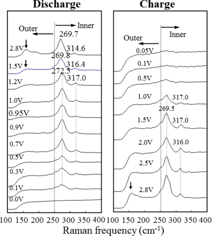
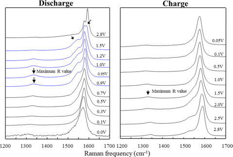
The decrease of intensity in all Raman lines for both samples (Figs. 12 and 13) upon doping with Li+ can be explained by three main behaviors: 1) in the region from 2.8 to 1.0 V, there exists a loss of the resonance conditions because of partial charge transfer; 2) at a potential of 0.9 V, the formation of an SEI->solid electrolyte interface film on the surface of the nanotube-electrode causes an abrupt step in the intensity of the TM of the inner tubes of DWCNTs (Fig. 13); and 3) as the potential decreases in the discharge process, the heavily doped Li+-nanotube system gives rise to highly increased electrical conductivity which results in reduced backscattering. The significant Raman changes observed in DWCNTs upon doping with Li+ resulted in complete depression of all Raman lines (e.g., RBM, TM, and G’ band), and may be associated with the outer tube experiencing a partial charge transfer of electrons to the nanotubes. Below a discharge potential of 1.0 V, the metallic inner tubes of the DWCNTs dominate all Raman lines, which is strongly supported by the appearance of full words please (BWF) profiles at around 1550 cm−1. It is suggested that the BWF coupling originates from the bundles of metallic tubes.
11.2. Hydrogen storage material
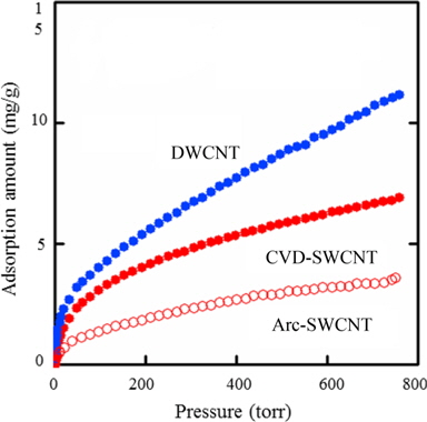
This section describes the hydrogen storing ability of DWCNTs as compared with that of SWCNTs [39]. Fig. 14 shows adsorption isotherms of supercritical H2 on a DWCNT and a SWCNT at 77 K. The DWCNT sample showed higher H2 adsorption ability than the SWCNT sample, even though the DWCNT sample has a specific surface area of 330 m2/g. Because the DWCNT has a well-ordered bundled structure, as seen from the TEM image, the interstitial pores can adsorb some H2 molecules, even though they appear to be too small for perfect accommodation of H2 molecules. As the g value increases, the interstitial volume becomes larger but the molecular potential fields become weaker.
It is well known that the basic properties of an impregnated catalyst are strongly affected by the impregnation method, the microstructure, the surface reactivity, and the metal precursor [40,41]. Among these factors, the morphology and nanostructure of the supports are considered to be the main factors with respect to obtaining a high dispersion of nano-sized particle catalysts. In this sense, DWCNTs are considered as preferred supporting materials for Pt catalysts. Li
11.4. Atomic force microscopy tips
Atomic force microscopy (AFM) has greatly contributed to the understanding and handling of nanometer-scale materials in recent years. To obtain better lateral resolution, carbon nanotubes are considered the preferred material for use as the probe tip of scanning probe microscopes on the basis of their large aspect ratio and good mechanical properties [43,44]. Even though SWCNTs are expected to provide good images including improved lateral resolution due to their small diameter (close to 1 nm), MWCNTs have provided better lateral images due to their good modulus [45,46]. It was reported that DWCNTs, having a similar diameter to that of SWCNTs and a comparable structural stability to that of MWCNTs, have been successfully attached to an AFM tip and then tested as a promising probe tip [47]. Interestingly, the fabricated DWCNT tip provided better high-resolution imaging than the conventional silicon tip or MWCNT tip, as well as a longer life time [47].
CNTs are considered preferred field emitters due to their large aspect ratio, chemical stability, high mechanical strength, and high electrical conductivity [48]. SWCNTs displayed excellent emitting performance [49], but readily degraded at high emission current [50]. In this context, DWCNTs have been examined as field emitting materials because they have a low threshold voltage comparable to that of SWCNTs and better structural stability compared to SWCNTs, being comparable to that of MWCNTs [51,52]. Hiraoka
11.6. Field-effect transistors
Integration of nanotube devices into circuits may become a reality in the near future, if we are able to produce carbon nanotubes with desired dimensions and properties [54,55]. In this context, DWCNTs could be ideal candidates for nanowires if they have a semiconductor-metallic configuration for the outer and inner constituent layers. Shimada
11.7. Reinforcing filler in polymer composites
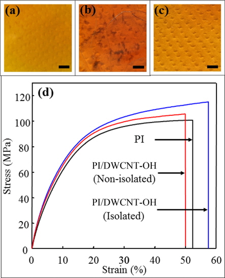
This section describes (DWCNTs) as a preferable reinforcing filler in polymers, under the conditions that they are individually isolated and have strong bonding strength with the given polymer [58]. Individually isolated DWCNTs were dispersed within a polyimide by combining suitable chemical modification and in-situ polymerization. DWCNTs possess superior mechanical properties and structural and thermal stability over SWCNTs. In addition, selectively introduced chemical moieties on the outer tubes provide lend dispersing ability to DWCNTs in organic solvents and effective anchoring sites for strong bonding strength with polymers, while sustaining optical and mechanical properties of the inner tubes of the DWCNTs. It is demonstrated that the individually dispersed DWCNTs within the polyimide, prepared by combining chemical modification of tubes and insitu polymerization process, contributed to the largely enhanced mechanical properties (i.e., 76% enhanced modulus, 42% improved tensile strength, and 71% greater elongation at break), thermal stability, and electrical properties of the polyimide while sustaining transparency (Fig. 15).
In this article, we have reviewed the synthesis, structure, physico-chemical properties, and promising applications of DWCNTs. While many ways of synthesizing DWCNTs have been reported, the dominant recent trend has been to synthesize DWCNTs using a catalytic CVD method, because this technique is known to be efficient in producing high-purity DWCNTs with small diameter distributions. However, a large amount of DWCNTs is required when considering specific applications (e.g., nanocomposites). In addition, the growth mechanism of DWCNTs relative to those of SWCNTs and MWCNTs should be better clarified, although plausible mechanisms have been suggested. The most challenging task is controlling their chirality during nanotube growth. Even though many other challenges must still be solved, extensive and intensive efforts in both academic and industrial research laboratories should soon overcome many of these barriers and the prospective role of DWCNTs in replacing SWCNTs and MWCNTs can be clarified for various industrial products.

![High resolution transmission electron microscopy (HR-TEM) images of (a) single-, (b) double-, (c) triple-, and (d) four-walled carbon nanotubes (CNTs, insets are their corresponding models). (e) Diameter distribution of catalytic chemical vapor deposition method-derived double walled CNTs based on detailed HR-TEM observations (total: 77). Note that their inner diameter of ca. 0.9 nm and outer diameter of 1.5 nm were below 2 nm. Reprinted from Kim et al. [10] with permission from Wiley-VCH.](http://oak.go.kr/repository/journal/13500/HGTSB6_2014_v15n2_77_f001.jpg)
![(a) Photographs of round and thin double walled carbon nanotube (DWCNT)-derived buckypaper (inset, thickness is ca. 30 μm). (b) Low-resolution transmission electron microscopy (TEM) image, and (c) field-emission electron microscopy images indicating a bundled structure. (d) Cross-sectional high resolution TEM image of a bundle of DWCNTs (inset is a schematic model, two concentric shells were regularly packed in a hexagonal array). (e) DWCNTderived buckypaper is flexible and mechanically strong enough to fold an origami. (f ) Semitransparent DWCNT-film on round cover glass (the characters in the acronym DWCNT are slightly blurred). Reprinted from Kim et al. [10] with permission from Wiley-VCH.](http://oak.go.kr/repository/journal/13500/HGTSB6_2014_v15n2_77_f002.jpg)
![(a) Low-frequency and (b) high-frequency Raman spectra for as-grown and purified double walled carbon nanotubes (DWCNTs), respectively, and (c) X-ray diffraction pattern (inset is stacking feature of DWCNTs). SWCNTs: single walled CNTs. Reprinted from Kim et al. [10] with permission from Wiley-VCH.](http://oak.go.kr/repository/journal/13500/HGTSB6_2014_v15n2_77_f003.jpg)
![(a) Low-frequency and (b) high-frequency Raman spectra for asgrown and thermally treated single walled carbon nanotubes (SWCNTs) and double walled CNTs (DWCNTs). Reprinted from Kim et al. [10] with permission from Wiley-VCH.](http://oak.go.kr/repository/journal/13500/HGTSB6_2014_v15n2_77_f004.jpg)
![(a) Adsorption isotherm of single walled carbon nanotubes (SWCNTs) and double walled CNTs (DWCNTs) (inset shows a comparative plot of the adsorption on both samples below P/P0 = 0.1), (b) micropore size distribution of SWCNTs and DWCNTs using the density functional theory method. The solid line indicates DWCNTs whereas the dotted line indicates SWCNTs. Note that small micropores below 0.8 nm corresponding to interstitial pores were observed in DWCNTs. Reprinted from Muramatsu et al. [12] with permission from Elsevier.](http://oak.go.kr/repository/journal/13500/HGTSB6_2014_v15n2_77_f005.jpg)
![Thermogravitic analysis of single walled carbon nanotube (SWCNT)- and double walled CNT (DWCNT)-derived buckypapers in an argon and oxygen (1%) gas mixture. It is noteworthy that improved oxidation stability in DWCNTs by ca. 200℃ is derived from their coaxial structure. MWCNTs: multi-walled CNTs. Reprinted from Muramatsu et al. [12] with permission from Elsevier.](http://oak.go.kr/repository/journal/13500/HGTSB6_2014_v15n2_77_f006.jpg)
![The photoluminescence maps (a) and intensities (b) of the SDBS- >sodium dodecylbenzene sulfonate-dispersed double walled carbon nanotube (DWCNT) and single walled CNT (SWCNT) suspensions in D2O. Reprinted from Shimamoto et al. [27] with permission from American Institute of Physics.](http://oak.go.kr/repository/journal/13500/HGTSB6_2014_v15n2_77_f007.jpg)
![Two-dimensional photoluminescence (PL) maps of the peapod grown double walled carbon nanotubes (DWCNTs) prepared at 1600℃, 1700℃, 1800℃, and 2000℃. The color represents the photoluminescence intensity on a linear scale shown on the right. The open circles show the locations of all peaks, where the values of n and m indicate the chirality of each nanotube. Note that there is no PL from arc-produced single walled CNTs due to their large diameters. Reprinted from Muramatsu et al. [28] with permission from Wiley-VCH.](http://oak.go.kr/repository/journal/13500/HGTSB6_2014_v15n2_77_f008.jpg)
![C1s X-ray photoelectron spectroscopy (XPS) (a) and F1s XPS (b) spectra of the double walled carbon nanotubes before and after fluorination at 200℃. Reprinted from Muramatsu et al. [29] with permission from The Royal Society of Chemistry.](http://oak.go.kr/repository/journal/13500/HGTSB6_2014_v15n2_77_f009.jpg)
![Low-resolution (a) and high-resolution cross-sectional (b) transmission electron microscopy (TEM) images of the pristine double walled carbon nanotubes (DWCNTs) and low-resolution (c) and high-resolution cross-sectional (d) TEM images of the fluorinated DWCNTs. Reprinted from Muramatsu et al. [29] with permission from The Royal Society of Chemistry.](http://oak.go.kr/repository/journal/13500/HGTSB6_2014_v15n2_77_f010.jpg)
![Low-frequency (a) and high-frequency (b) Raman scattering of the double walled carbon nanotubes before and after fluorination at 200°C. Reprinted from Muramatsu et al. [29] with permission from The Royal Society of Chemistry.](http://oak.go.kr/repository/journal/13500/HGTSB6_2014_v15n2_77_f011.jpg)
![Low-frequency Raman spectra of the double walled carbon nanotubes during the discharge and charge processes. Reprinted from Kim et al. [38] with permission from Wiley-VCH.](http://oak.go.kr/repository/journal/13500/HGTSB6_2014_v15n2_77_f012.jpg)
![High-frequency Raman spectra of the double walled carbon nanotubes during the discharge and charge processes. Reprinted from Kim et al. [38] with permission from Wiley-VCH.](http://oak.go.kr/repository/journal/13500/HGTSB6_2014_v15n2_77_f013.jpg)
![The H2 adsorption isotherms of single walled carbon nanotubes (SWCNTs) and double walled CNTs (DWCNTs) at 77 K. CVD: chemical vapor deposition. Reprinted from Miyamoto et al. [39] with permission from American Chemical Society.](http://oak.go.kr/repository/journal/13500/HGTSB6_2014_v15n2_77_f014.jpg)
![Visual appearances of pure polyimide (a), non-isolated double walled carbon nanotubes (DWCNTs)/polyimide (b), and isolated DWCNTs/ polyimide (c) films; note that film transparency strongly depends on dispersion quality. d) Typical stress-strain curves of pure polyimide and chemically modified DWCNT-reinforced polyimide films. Scale bars (a-c): 1 cm. PL: photoluminescence. Reprinted from Jung et al. [58] with permission from Wiley-VCH.](http://oak.go.kr/repository/journal/13500/HGTSB6_2014_v15n2_77_f015.jpg)