Zinc oxide varistor is a multicomponent semiconductor device, which is made by sintering zinc oxide doped with main subordinate metal oxides, such as bismuth, praseodymium, or vanadium, and secondary subordinate metal oxides, such as cobalt, antimony, manganese, and chrome. Zinc oxide varistor reveals a distinctive microstructure of SIS type, composed of Semiconductor (zinc oxide grain)-Insulator (intergranular layer)-Semiconductor (zinc oxide grain), by the sintering process. Zinc oxide varistor can be considered as a multi-junction device, composed of many series and parallel connections of grain boundaries [1-4]. As a result, zinc oxide varistor shows electrical characteristics that are similar to back-to-back zener diode, which exhibits highly nonlinear properties above a threshold voltage. Therefore, zinc oxide varistor is usefully utilized as a core element of surge absorbers, to protect electronic and electrical circuits from overvoltage; and as a core element of surge arresters, to protect electric power systems from lightning surges [2-5].
The microstructure and electrical properties of zinc oxide varistor ceramics can be modified by the addition of various metal oxides. It is well known that the co-addition of praseodymium and cobalt to pure zinc oxide essentially induces nonlinear properties from ohmic properties, in the voltage-current relation [6-10]. The addition of various rare earth oxides can noticeably increase the breakdown field, and improve the nonlinear coefficient [11-13]. Nahm et al. reported that the zinc oxide varistors composed of Zn-Pr-Co-Cr(ZPCC)-R2O3 (R = Er, Y, Dy, etc.) have highly nonlinear properties, and high stability against various stress [14-17]. ZPCCR varistors are based on the quinary system in ceramic composition. The sinterability of the quinary system ZPCCY, added with a small content of aluminum, was enhanced, even at temperature as low as 1,280℃; in addition, it showed high stability against accelerated aging stress [18]. In order to apply wide band applications, it is very interesting to explore the roles and combinatory effect of the additives. The effect of erbium on the electrical properties of ZPCC-based varistors added with aluminum has seldom been reported. In this work, the aim is to investigate the effect of the content of doped erbium on the microstructure and electrical properties of the senary system ZPCCAE (Al2O3-Er2O3).
ZPCCAE varistor samples were prepared from a mixture of (97.995-x) mol% ZnO, 0.5 mol% Pr6O11, 1.0 mol% CoO, 0.5 mol% Cr2O3, 0.005 mol% Al2O3, and x mol% Er2O3, where x ranges from 0 to 2.0. Raw materials were mixed by ball milling with zirconia balls and acetone in a polypropylene bottle for 24 h. The mixture was dried at 120℃ for 12 h, and calcined in air at 750℃ for 2 h. The calcined mixture was pulverized using an agate mortar and pestle, and after 2 wt% polyvinyl alcohol (PVA) binder addition, granulated by sieving through a 100-mesh screen, to produce the starting powder. The powder was uniaxially pressed into diskshaped pellets of 10 mm diameter and 2 mm thickness, at a pressure of 100 MPa. The pellets were sintered for 1 h at 1,300℃, and furnace-cooled to room temperature. The heating and cooling rates were 4℃/min. The sintered pellets were lapped and polished to 1.0 mm thickness, using a lapping/polishing machine (GLP-S20/25; GLP Korea, Geumchun-Gu, Seoul, Korea). The final samples were about 8 mm diameter, and 1.0 mm thickness. Silver paste was coated on both faces of the varistor samples, and the electrodes were formed by heating it at 550℃ for 10 min. The electrodes were 5 mm in diameter. Finally, after the lead wire was soldered to both electrodes, the varistor samples were packaged, by dipping them into a thermoplastic resin powder.
2.2 Microstructure examination
Both surfaces of the sintered pellets were lapped and ground with SiC paper, and then polished with 0.3 μm-Al2O3 powders to a mirror-like surface. The polished samples were thermally etched at 1,050℃ for 20 min. The surface microstructure was examined by scanning electron microscopy (FESEM, Quanta 200, FEI, Brno, Czech). The average grain size d was determined by the lineal intercept method, given by d= 1.56 L/MN, where L is the random line length on the micrograph, M is the magnification of the micrograph, and N is the number of grain boundaries intercepted by the lines [19]. The compositional analysis for minor phases was carried out by energy dispersion X-ray spectroscopy (EDS) attached to the SEM unit. The crystalline phases were identified by X-ray diffractometry (XRD, X'pert-PRO MPD, Panalytical, Almelo, Netherlands) with CuKα radiation. The sintered densities ρ of pellets were measured using a density determination kit (238490) attached to a balance (AG 245, Mettler Toledo International Inc., Greifensee, Switzerland), with deionized water as a liquid medium.
The electric field-current density (E-J) characteristics were measured, using a high voltage source-measure unit (Keithley 237, Keithley Instruments Inc., Cleveland, OH, USA). The breakdown field EB was measured at 1.0 mA/cm2, and the leakage current density JL was measured at 0.8 EB. In addition, the nonlinear coefficient α is defined by the empirical law, J= K·Eα, where J is the current density, E is the applied electric field, and K is a constant. α was determined by the following expression [1]: α = (logJ2-logJ1)/ (logE2-logE1), where J1= 1.0 mA/cm2, J2= 10 mA/cm2, and E1 and E2 are the electric fields corresponding to J1 and J2, respectively.
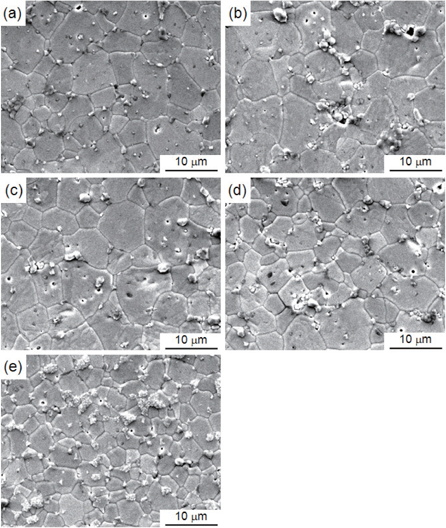
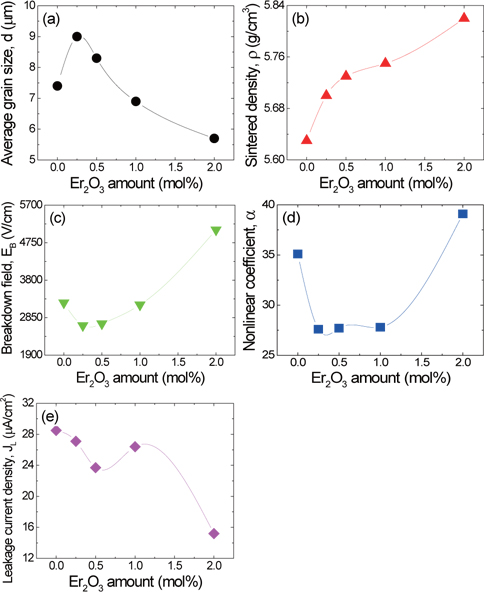
Figure 1 shows SEM micrographs of the varistor samples for different erbium amounts. Outwardly, the microstructure of the varistor samples consisted of ZnO grain (blackish part) as a primary phase, and intergranular layer (whitish part) as a minor secondary phase [4,8,13]. The secondary phase was found to locate at grain boundaries, nodal points, and occasionally within the grains. In addition, the secondary phase amount increased with the increase of the doped erbium amount. The detailed microstructure parameters are summarized in Table 1. The average grain size α as a function of the erbium amount is shown in Fig. 5(a). The average grain size d increased from 7.4 to 9.0 μm when the erbium amount was increased up to 0.25 mol%, and then decreased when it was further increased from 0.25 and 2.0 mol%. The decrease of average grain size d is attributed to the increase of the secondary phase amount at the brain boundaries and the nodal points. As a result, the doped erbium acted as a grain growth inhibitor, at an amount exceeding 0.25 mol%. The densities ρ of sintered pellets as a function of the erbium amount are shown in Fig. 5(b). The density ρ increased from 5.63 to 5.82 g/cm3 (5.78 g/cm3 in pure ZnO) with the increase of the erbium amount, and it was very dense, with almost no porosity. These ceramics were obviously improved in terms of the densification and uniformity of grain size in the microstructure, despite sintering at 1,300℃, compared with ZPCCE ceramics sintered at 1,350℃, with no Al2O3 [13]. This showed the obvious effect of the minor addition of Al2O3.
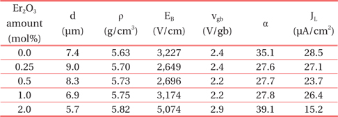
Average grain size (d), sintered density (ρ), breakdown field (EB), breakdown voltage per grain boundary (vgb), nonlinear coefficient (α), and leakage current density (JL) of the varistor samples, for different erbium amounts.
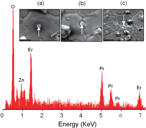
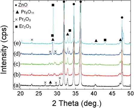
Figure 2 shows XRD patterns of the varistor samples for different erbium amounts. The samples revealed two phases. The bulk phases were a polycrystalline matrix of ZnO doped with extremely small amounts of minor additives. The intergranular phases were mixture phases composed of praseodymium and erbium, and formed the secondary phases. No phase related to Er2O3 was detected. The secondary phases are clearly distinguished from the ZnO bulk phases indicated in the SEM micrograph. The EDS analysis in Fig. 3 shows that the praseodymium and erbium are mainly segregated at grain boundaries and nodal points, because of much larger ionic radius than that of zinc, and coexisted at the grain boundaries and the nodal points, as if they were a single phase.
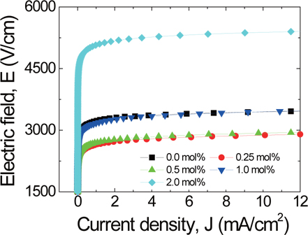
Figure 4 shows the E-J characteristics of the varistor samples for different erbium amounts. The electrical conduction shows a voltage-switching curve, which divides into nonconduction (linear region), due to extremely high resistance, and conduction (nonlinear region), due to extremely low resistance. In a linear E-J relation, the predominant nonconduction mechanism is a thermally assisted thermionic emission over the Shottky potential barrier, before the critical operation field (EB). In a nonlinear E-J relation, the predominant conduction mechanism is a Fowler-Nordheim field emission (quantum mechanic tunneling), through a Shottky potential barrier. These nonlinear properties are attributed to a distinctive microstructure, in which the grain boundaries between ZnO grains accompany a potential barrier.
The behavior of the breakdown field EB as a function of the erbium amount is shown in Fig. 5(c). With the increase of the doped erbium amount, the breakdown field EB decreased, until the doped erbium amount was 0.25 mol%. The minimum breakdown field EB was 2,649 V/cm. When the doped erbium amount exceeded 0.25 mol%, the breakdown field EB increased again. When the doped erbium amount was in the range of 0.25 to 0.5 mol%, the doped erbium amount had little effect on the breakdown field EB. The main factors that affect the breakdown field EB are the grain size d, and the breakdown voltage per grain boundary vgb. The breakdown voltage VB is indicated as the following expression [2], VB = (D/d)·vgb = n·vgb. Therefore, the breakdown field EB is written as follows: EB = vgb/d, where d is the average grain size, D is the thickness of sample, and n is the number of grain boundaries. In general, the breakdown voltage can be mainly controlled by the varistor sample thickness for fixed grain size, and subordinately by the grain size for constant sample thickness. As a result, the increase of the breakdown field EB with the increase of the doped erbium amount is strongly attributed to the decrease of the average ZnO grain size.
The behavior of the nonlinear coefficient α as a function of the erbium amount is shown in Fig. 5(d). With the increase of the doped erbium amount, the nonlinear coefficient α decreased, until the doped erbium amount was 0.25 mol%. The minimum nonlinear coefficient α was 27.6. When the doped erbium amount exceeded 0.25 mol%, the nonlinear coefficient α increased again. The nonlinear coefficient α increased in a very small extent when the doped erbium amount increased in the range of 0.25 to 1.0 mol%. In fact, the doped erbium amount had little effect on the nonlinear coefficient α, in the range of 0.25 to 1.0 mol%. The nonlinear coefficient α obtained the maximum value of 39.1 when the doped erbium amount was 2.0 mol%.
The behavior of the leakage current density JL as a function of the erbium amount is shown in Fig. 5(e). With the increase of the doped erbium amount, the leakage current density JL almost did not vary, until the doped erbium amount was 1.0 mol%. The minimum leakage current density JL was 15.2 μA/cm2 when the doped erbium amount was 2.0 mol%. On the whole, the leakage current of these varistor samples exhibited high values, compared with other praseodymium-doped ZnO varistors [13-17]. However, the leakage current density JL of the Al2O3-free Prdoped ZnO varistors was not so high. Therefore, the high leakage current density JL in this system may be related to the combinatory effect of Al2O3 and Er2O3, whereas it not clear at present.
This study investigated how the doped erbium amount affects the microstructure and varistor properties of ZPCCAE (ZnOPr6O11-CoO-Cr2O3-Al2O3-Er2O3) ceramics. The ceramics showed a simple microstructure, which consisted of ZnO grains and intergranular layers. The erbium additive significantly contributed to the densification, and acted as an inhibitor of grain growth. The erbium additive increased the breakdown field, due to the decrease of average grain size. The effect of the erbium amount on the nonlinear coefficient exhibited the peculiar phenomenon of a U-shaped curve, as the amount of doped erbium increased. The increase of the doped erbium amount reduced the leakage current density.