Thin films have been increasingly used in the optics, semiconductors and material industries to provide specific functions to the coated devices. Effective measurement of the profile and the film thickness are important to achieve special functions. To measure the thickness and surface, optical methods such as white-light interferometry and reflectometry have been widely used. Recently, white light scanning interferometry has extended its application from the surface measurement to the thin film thickness measurement. However, due to the phase distorting effect of the transparent thin-film, it is very difficult to measure a transparent thin-film on the top of the 3-D surface by conventional metrology.
Reflectometry is more popular in industries for its fast throughput. Reflectometry is a well-established and powerful technique for measuring film thickness [1, 2]. It measures reflectance for different wavelengths to calculate thickness. But, this technique can only determine the film thickness and it is limited to only one point detection. Recently, volumetric thickness profile has been measured using a CCD camera [3].
To measure the 3-D profile of a transparent surface, a white light interferometry technique which gets spectrally resolved analysis by Fourier transform was proposed [3-4]. It determines both surface profile and film thickness in the spectral domain. Kim’s method extracted thickness information from the interferogram. It has the merit that it does need additional spectral units, but spectral information usually is not enough for calculating the thickness in a practical measurement. And it has the limitation of spectral resolution, which is most important in calculating thickness. To compensate for the ambiguity in spectral analysis, reflectometry and spectrally resolved white light interferometry were combined [5, 6]. But this method was too sensitive to the detection of the peak signal. Modeling based researches also had been proposed recently [7-10]. And several researchers have used different techniques to measure the thin film thickness and height accurately [11-20]. However, there still remains ambiguity in detecting surface height due to the thin film effect. They had practical limitations of uncertainty and measurement speed. To overcome those problems we have combined a spectrometer into an interferometry system. As a result, the proposed method can gather more accurate and highly resolved spectral information for thickness calculation.
In this paper we combine the white light scanning interferometry and reflectometry for determination of film thickness and surface profile. The key idea is to divide the measurement into two states, reflectometry mode and interferometry mode, to get the two unknowns of thickness and surface profile separately. The experiment was performed in two steps. First the film thickness was determined in reflectometry mode. For the next step, the thickness and surface profile are calculated by white light scanning interferometry mode using the thickness value which is determined by reflectometry mode. It saves calculation time for least-square fitting because it does not need an initial guess for the thickness value. For reflectometry mode, a normal objective lens and spectrometer were used to measure the thickness of the specimen. For interferometry mode, an interferometric lens (mirau type) and CCD sensor were used to measure the film thickness and surface profile. The shape and position of an interferogram varies depending on several parameters such as the height and thickness of the specimen. And it can be modeled using the theory of interferometry and reflectometry. The optimum model provides the surface profile and the thin-film thickness simultaneously. The final thin-film and surface profile were measured by obtaining the best matching model using the non-linear least square fitting. For the interferometry mode, we considered the phase changing effect of the thin-film on the top of the surface for accurate and simultaneous measurements of the film thickness and surface profile.
By separating the thickness measurement from the surface profile measurement using reflectometry, we enhanced the accuracy of both surface profiling and thickness measurement. The most important advantage of the proposed technique is the elimination of the ambiguity in determination of thickness and surface by separating measurement of thickness and surface profile.
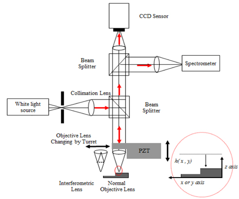
The experimental setup is shown in Fig. 1. A vertical movement in the z direction was implemented using the piezoelectric actuator toward the test surface located in the x-y plane. The test surface is observed through objective (Nikon ELWD 10X/20X/50X) lenses and an interferometric (Nikon 20X/50X Mirau type) objective. The light source is a halogen lamp with a broad and continuous spectrum.
The setup can be used both for reflectometry measurement mode or interferometry measurement mode. When it uses a normal objective lens and spectrometer, it does not allow the light reflected on the reference surface to reach the spectrometer because a normal objective lens does not have a reference mirror inside. So, under this condition, the spectrometer records interference between the top and bottom surface of the film in the specimen. This is known as reflectometry mode. When the interferometric lens and the CCD camera were used, the light reflected on the reference surface. The reflection interfered with the test surface beam. Now the CCD camera records the interference signal between the test and reference signals. This mode is known as white light interferometery mode. In this mode, the interferogram gives information about the thin film thickness
For the measurement of reflectometry mode, the spectrometer (Ocean Optics QE65000; 1024 pixels), which has a detecting range from 200 nm to 1100 nm, was used. The spectrometer is aligned at the center of the camera so that the light reflected from the center of the specimen can enter the spectrometer. By implementing a normal objective lens and 50
For the measurement of interferometry mode, the interferometric objective was fitted with a PZT. The control voltage to shift the PZT for phase shifting was produced by a Micom with PID control. The camera (Vieworks VG264, 250 fps) gives an 8-bit digital output. The interferograms were transferred to the PC through an image acquisition board.
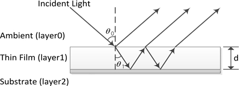
When incident light is upon a surface with a transparent thin-film layer, multiple reflection takes place, as illustrated in Fig. 2. If we take account of the multiple reflections inside the transparent thin film layer, the parameter R (total reflection coefficient) can be derived as Eq. (1) [1]

where

where

Considering the reflection of the specimen, interference signals can be expressed as a sum of reference light and objective light as,


where, z is the position of PZT, k is the wavenumber, Eref(z,k) is the wave equation of reference light, Eobj(z,k) is the wave equation of measurement light. ρ is the reflection coefficient of the beam splitter, |
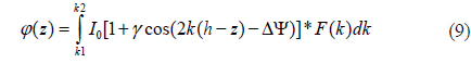
Considering incoherent superposition of monochromatic lights, the interference intensity sampled from a surface point (x,y) of height h is generally described as the integral of the effective wave number from

where
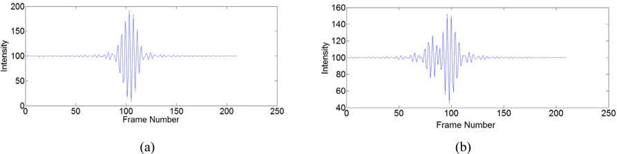
In the case of Fig. 3(a), the psi of the sample does not vary because there is no thin-film on the top layer. In the case of 3(b), the interference of the top layer is affected by the signal from the bottom surface. As the thin film gets thinner, the interference signal of the bottom surface affects the interference signal of the top surface.
3.3. Non-linear Least Square Fitting
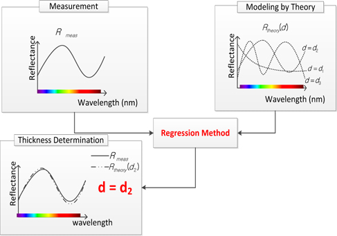
In reflectometry mode, after the data acquisition process is completed, a regression method, such as the Levenberg-Marquardt non-linear fitting algorithm, is used for searching the best-matching theoretical reflectance. The aim of the fitting process is to find the thin film thickness that minimizes the difference between the measured reflectance and the theoretically calculated reflectance. In order to evaluate the difference, the error, e(d), in Eq.(10) is used. The difference is squared and integrated in wavelength range. As the error gets close to zero, the theoretical reflectance gets more similar to the measured reflectance.
In interferometry mode, surface height
The optimum model shows the surface profile
The experiment was performed in two steps. First, thin film thickness was determined in reflectometry mode and then the film thickness and the surface profile was calculated by interferometry mode. For interferometry measurement, the thickness value determined by reflectometry mode was used as the initial thickness value
4.1. Reflectometry Mode Result
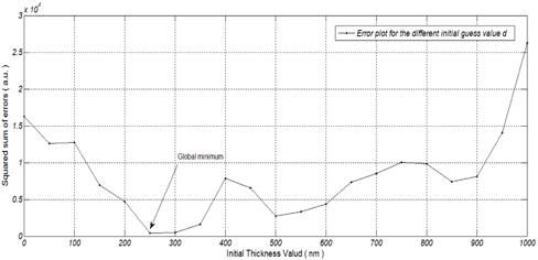
A regression method like Levenberg-Marquardt nonlinear fitting algorithm is used for searching for the best-matching theoretical reflectance. The aim of the fitting process is finding the thickness of thin film which minimizes the difference between measured reflectance and theoretically calculated reflectance. The procedure of finding the best matching model is shown in Fig. 4.
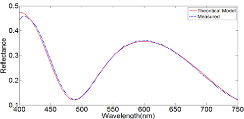
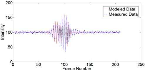
Using the reflectometry mode, the proposed reflectance and phase modeling was verified. SiO2 film of 408 nm thickness was deposited on a Si substrate by NIST; NIST 400-100, CRADA, CN-1364, 19984. Figure 5 shows the fitting result between the measured reflectance signal and modeled reflectance signal. We searched for the optimal thickness of the film thickness ‘
4.2. Interferometry Mode Result
The thickness ‘
To verify the effectiveness of the interferogram modeling, reference specimens which have SiO2 film layers on silicon have been analyzed; NIST reference specimen for 408 nm (NIST 400-100, CRADA, CN-1364, 19984) and Mikropack-ID0076 specimen for the others (from 40 nm to 1000 nm).
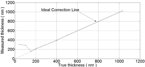
To verify the performance of the proposed technique, samples of thickness lower than 200 nm also have been investigated. Fig. 7 shows the comparison of the true value and measured thickness value. When the thickness is lower than 150 nm, correct measurement result is not guaranteed; it shows the limitation of the proposed method. The reason for the limitation is when the deposited film gets thinner than 150 nm, thicknesses can no longer be distinguished from one to the other because the phase change within the thin-film layer becomes very small regardless of wave number when thickness
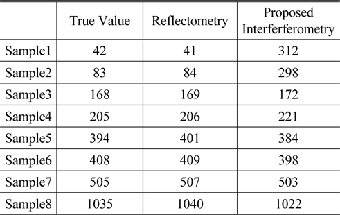
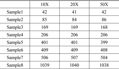
For verifying proposed reflectometry, we measured samples in Table 1 using three objectives with different magnification. The test result indicates that the maximum deviation reaches; 0.6% when the thickness value is in the range 350 nm- 1100 nm. It shows enhanced thickness measurement accuracy compared with previous research; 3% [4]
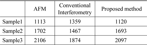
[TABLE 1.] Comparison of sample thicknesses measured by two methods (unit : nm)

Comparison of sample thicknesses measured by two methods (unit : nm)
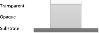
The thin-film-transistor (TFT) supporting structure, which is a very important structure in the Liquid Crystal Display panel illustrated in Fig. 8, was measured by using the proposed method for industrial application. The sample has two layers from the bottom. The first layer is relatively thick with opaque material and the second layer consists of transparent thin film. These kinds of samples could be measured to evaluate the performance of the proposed method. Table 3 shows the measured results for the sample shown in Fig. 8. AFM measurement results are also provided in Table 3 for comparison. The conventional bucket algorithm by Larkin [17] gave a different value from the true value due to the thin-film effect on the top of the surface. On the other hand, the proposed method showed a maximum difference of 9 nm from the AFM results. Accuracy of the conventional method is not guaranteed when transparent film exists; 22.1% error (Table 3). On the other hand the proposed method showed enhanced accuracy; 0.7%. It shows enhanced surface measurement accuracy compared with previous research; 3% [4].

Comparison of sample thicknesses measured by reflectometry mode with three objectives (unit : nm)
[TABLE 3.] Comparison between the conventional method and the proposed method (unit: nm)
Comparison between the conventional method and the proposed method (unit: nm)
In searching for the true values of
For verifying proposed methods, we measured samples of Table 2 using two objectives with different magnification. The test result indicates that the maximum deviation reaches; 0.5% when the magnification varies from 20X to 50X (Table 4).
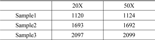
Comparison of sample heights measured by interferometry mode with three objectives (unit: nm)
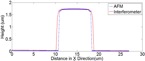
The profile of the sample was compared with the AFM measurement result, as shown in Fig. 10.
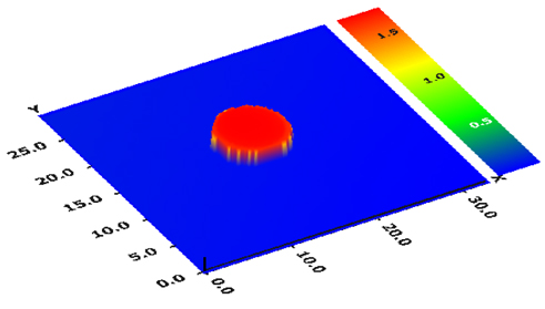
The comparison showed fairly good matching profile. Finally, a 3-D surface profile measured using the proposed algorithm is shown in Fig. 11.
White light scanning interferometry is a well-established technique in surface profiling applications. The resolution in this technique is of the order of a nanometer. But when a transparent thin film exists, the reflection signals from both the top and bottom surfaces of the film will interfere with the reference signal. At the same time, the multiple reflection signals between the two film surfaces will also interfere with the others. Effective separation of the interference signals from each other is the key to achieving a successful measurement. In this paper, measurement of the surface profile and thin-film thickness by interferometry combined with reflectometry was proposed. The key idea is to divide the measurement into two states using reflectometry mode and interferometry mode to obtain the two unknowns separately; thickness
The maximum difference between the measured height and the reference height was more than 250 nm under the conventional bucket algorithm, but the difference was reduced to 16 nm under the proposed method. Accuracy has been enhanced from 22.1% to 0.7% for height measurement using the proposed method. The modeling method was more effective when it was used for a thin-film (< 1 μm) because the phase distortion of the thin-film gets worse as the thin film gets thinner. The AFM profile showed a fairly good matching result with the profile of the proposed method. This technique is available not only probing the thickness point by point but also providing complete volumetric film profiles digitized in three dimensions. At present, this measurement technique provides nanometer resolutions of the vertical height when the transparent film thickness exceeds 150 nm. The limitation occurs when the deposited film gets thinner than 150 nm. The reason is that the interferogram can no longer be distinguished from one to the other because the phase change within the thin-film layer becomes very small regardless of the wave number when thickness d is small. A more rigorous reflection model is required to improve a measurement accuracy lower than 150 nm. In conclusion, the most important advantage of the proposed technique is the elimination of the ambiguity in determining the thickness and surface profile. By separating measurement of thickness and surface profile, the proposed method effectively eliminated the ambiguity of thickness determination.