Research and development of GaN-based light emitting diodes (LEDs) have grown rapidly in the last decades due to their promising applications such as back light units for flat panel display, signage, and general lighting [1]. Commercial blue and green LEDs employing InGaN/GaN multiple quantum wells (MQWs) are now available [2]. However, there still are a lot of problems that need to be solved in order to achieve the high-efficiency and high-brightness LEDs that are expected to be widely used for general lighting technology instead of conventional light sources such as incandescent and fluorescent bulbs. For example, because of the total internal reflection, only a small fraction of the light generated in the active region of the LED can escape to the surrounding air, resulting in a low external quantum efficiency even if the internal quantum efficiency of the InGaN/GaN LED has been improved substantially by the advanced epitaxial growth techniques [3]. This problem can also be resolved by introducing several techniques such as chip sidewall, surface roughening, patterned substrate, graded-refractive-index coating, and photonic crystal technologies [3, 5]. Photonic crystal LED is considered to be a promising approach because it is believed to improve the light extraction efficiency of the LED in two ways. One is the use of the photonic band gaps made by photonic crystal to prevent the guided modes emissions; only light generated in the band gap region can radiate outward since lateral propagation of the guided modes are prohibited in the band gap, thus improving extraction efficiency [5, 6]. The other consists in using photonic crystal to couple the guided modes to radiative modes and diffract those to the air [7, 8].
Because of the chemical stability of the GaN material, a dry etching technique such as inductively coupled plasma reactive ion etching (ICP-RIE) is usually employed to fabricate the photonic crystal structures on the InGaN/GaN LEDs. Theoretically, the higher light extraction efficiency of the LED is expected from the deeper photonic crystal pattern regardless of the bandgap or the non-bandgap structures [8]. However, the experimental results reveal that light emission intensity is usually reduced when the etched-patterns penetrate into the MQW active layer due to the plasma-induced damage [9, 10]. Therefore, most of the studies using photonic crystal for the InGaN/GaN LEDs focus on the patterning just on their top p-GaN layer. In this paper, we report on the improvement of cathodoluminescence (CL) of the InGaN/GaN blue LEDs with deep nano-hole arrays, which are penetrated into the MQW regions, fabricated using a combination of the ICP-RIE and wet chemical etching. The dry etching process allows the fabrication of the deep nano-patterns, while the wet chemical etching process is supposed to recover the plasma-induced damage and increase the sidewall areas of the nano-holes, which significantly contribute to the enhancement of the light extraction efficiency of the LED. In addition, we employ a CL mapping technique to investigate the light emission profile from the nano-patterned LEDs. Compared to other optical characterizations such as photoluminescence or electroluminescence, the CL mapping technique has advantages due to the fine probing capability of the electron beam.
The InGaN/GaN blue LED with a light emission peak at around 430 nm has been grown by low-pressure metalorganic chemical vapor deposition (LP-MOCVD) on a sapphire (0001) substrate. The LED structure is composed of GaN-based double heterostructures, which includes, from the bottom, a 1-μm-thick undoped GaN layer grown on a low-temperature nucleation layer, 4-μm-thick Si-doped n-GaN layer, six In0.3Ga0.7N/GaN MQWs with well and barrier thickness of 3 and 7 nm, respectively, and a Mg-doped p-GaN top cladding layer of 200 nm. To fabricate the photonic crystal structure, the LED wafer is coated with 300-nm-thick electron beam resist (ZEP-500A). The two dimensional square lattice photonic crystal patterns with circular holes are created by electron beam lithography (JBX 9300FS, JEOL). The diameter and periodicity of the circular holes are intentionally chosen to be 200 and 500 nm, respectively. The samples are then etched by an ICP dry etcher (MULTIPLEX ICP, STS) using a mixture of BCl3 and Cl2 under the ICP source power of 800 W and the RF bias power of 100 W. Under these conditions, the etching rate for GaN is measured to be about 5 nm/s. The ICP etching time is varied to investigate the influences of etching depths on the light emission efficiency of the blue LEDs. After the cleaning process, the samples are divided into two sets. One is used for the CL measurements and the other is transferred to the wet etching process. For the latter, the patterned LEDs are dipped into a 4-M KOH solution at 50℃ for 20 mins. The InGaN/GaN wafer without a photonic crystal structure, that has undergone the same processes, is used as a reference for the CL measurements. Morphology and etching depth of the photonic crystal structures are investigated by a field-emission scanning electron microscopy (FE-SEM) and a focused ion beam (FIB) technique. The CL measurements are carried out at room temperature using a 10-kV e-beam with a Gatan MonoCL3 system equipped with a high-sensitivity photo multiplier tube (PMT) attached to an SEM (S-4300SE from Hitachi). With this energy, the electron beam penetrates the GaN layer by about 0.7 μm with a quite broad energy deposition profile [11]. There are two ways in obtaining a CL signal from the specimen. One is panchromatic CL images in which the images are formed by plotting integrated luminescence of the wavelength range (160~930 nm) of the PMT detector at each point of the electron beam irradiation. The other is monochromatic CL images that only luminescence at particular wavelength is plotted by adjusting the spectrometer. All the CL images of the samples presented in this study are monochromatic images that are recorded at the wavelength corresponding to the emission peak of the InGaN/GaN MQWs.
We first study the CL of the patterned LEDs after the ICP etching process with different etching depths. It reveals that all of the patterned LEDs showed a higher CL intensity compared to that of the as-grown LED. The enhancement of the CL intensity is increased with increasing etching depth, achieved a maximum 2-fold higher value at a depth around 150 nm and then decreased when the etching depth is deeper than this value. This CL enhancement trend of the patterned LED is reasonable because the thickness of the p-GaN layer in our InGaN/GaN LED is about 200 nm. Higher light extraction efficiency is expected at the deeper etching depth because more guided-modes in the LED structure are expected to have the opportunity to be diffracted to the air [8]. However, when the hole patterns come too near to or penetrate into the MQW layers, the high-energy ICP-RIE process can induce plasma damage effects that can degrade the emission property of the MQW active layer; this may be attributed to the observed CL intensity reduction from the deep-patterned LEDs.
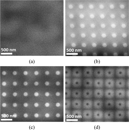
Figure 1 shows the CL mapping images of the LEDs without and with nanohole arrays fabricated by ICP-RIE with etching depths of about 100, 150, and 250 nm. Note that these monochromatic CL images are recorded at the MQW peak emission wavelength. A non-uniform luminescence profile observed in the planar LED as in Fig. 1(a) may be due to the inhomogeneous In distribution in the InGaN/GaN MQWs and/or well thickness variation [12]. Interestingly, spatial distribution of the luminescence around the nanoholes is observed to be distinctively different in the two cases. In the case of the etched holes within the p-GaN layer [see Figs. 1(b) and 1(c)], light emission intensity inside the nanoholes is much stronger compared to that at the unpatterned regions as demonstrated by the bright spots in the CL images. When the etching depth penetrates into the MQW layers [see Fig. 1(d)], the light emitted from the MQWs is scattered only at the sidewalls of the nanoholes, and bottom regions of the nanoholes are observed as dark spots in the CL mapping images. It is worth noting that the soft mask (ZEP-500A) used for the fabrication of the photonic crystal patterns is also slightly etched out during the ICP-RIE process. Therefore, the circular hole patterns tend to become a truncated-inverted-cone (TIC) shape when transferred to the LEDs after relatively long etching time. Experimentally, it is difficult to fabricate a perfect two-dimensional photonic crystal structure with a photonic bandgap for the InGaN/GaN blue LED. In addition, it is argued that the enhanced light extraction from the LEDs with the photonic crystal is mainly due to the light scattering by individual nano-holes rather than the photonic crystal band structure [13-14]. In this study, we chose a quite small value of radius/lattice constant ratio of the air holes (r/a=100/500=0.2) for our photonic crystal structure. This value is located beyond the region that is expected for a photonic bandgap related with the blue light [15]. By using a small r/a value, we may be able to fabricate the TIC shaped deep nanoholes that are quite effective for the light extraction of the InGaN/GaN LED due to the enhanced light scattering at the inclined-inner-surface of the etched holes [16-17]. The observed reduction of the CL intensity of the patterned LEDs with the deep nanoholes is mainly caused by plasma-induced damages rather than the removal of active material. It is known that during the dry etching processes of the GaN using ICP-RIE, the surface potential change may induce defects such as nitrogen vacancies and other surface oriented defects on the etched surfaces [18]. These result in a degradation of the electrical and optical characteristics of the InGaN/GaN LED. It is known that the plasma-induced damages on the surfaces may be recovered by annealing or chemical treatments [9, 10, 18]. In this study, we investigate the effect of KOH wet chemical treatment on the luminescence properties of the e-beam nano-patterned InGaN/GaN LED, especially when the nano-patterns penetrate into the MQWs.
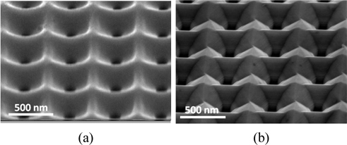
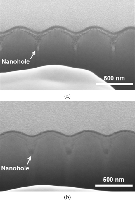
Figure 2 shows SEM images of the 250-nm deep nano-hole arrays fabricated by the ICP etching (a) before and (b) after wet chemical treatment for 20 mins in the KOH solution. It reveals that, after the wet etching processes, the nanoholes are widened and tend to have an improved hexagonal symmetry. It is worth noting that the hole depth change is observed to be negligibly small, which is consistent with the facts that the GaN (0001) plane is chemically inert and that the GaN material has anisotropic etching properties, for which the etching rate is quite different for different crystal planes [19, 20]. To observe inside the deep nano-hole arrays, we carry out cross-sectional SEM measurements using a dual-beam focused ion beam system (FIB-Nova600, Nova Lab). A thin Pt layer is deposited on the sample surface to protect LED epilayers from ion-induced damages and then cross-sectional images are observed by SEM after patterning with an ion beam. Figures 3(a) and 3(b) show cross-sectional SEM images of the 250-nm deep nanoholes before and after KOH etching, respectively. One can clearly see that inner side walls of the nanoholes are quite rough and the residues appear at their bottom after the ICP etching process [Fig. 3(a)]. After KOH etching, in contrast, the side walls are smooth and almost no residues are observed inside the nanoholes as can be seen in Fig. 3(b).
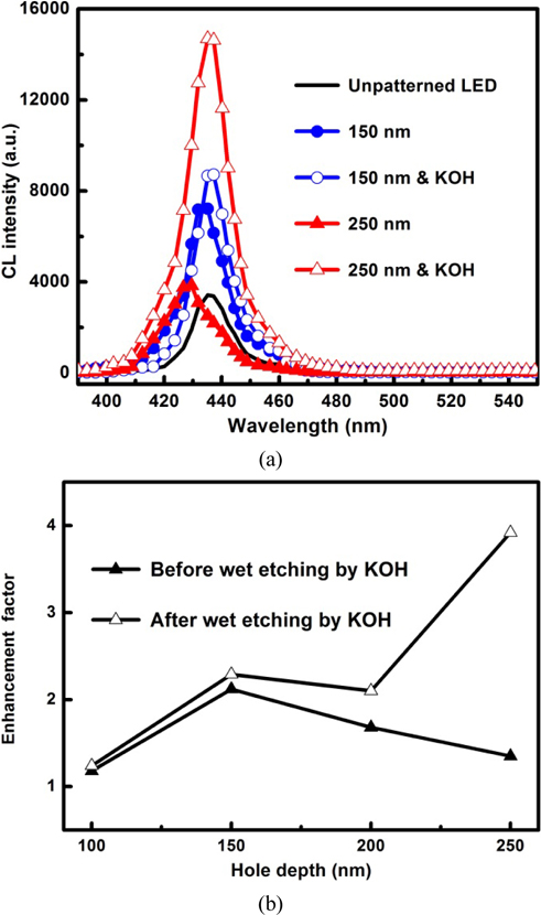
Figure 4(a) shows the CL spectra of the LEDs with shallow (150-nm) and deep (250-nm) nanohole arrays before and after KOH treatments. The blue emission peak of the patterned LEDs is slightly shifted to a shorter wavelength compared to that of the unpatterned sample after the ICP etching process. After KOH treatment, the emission peaks tend to be recovered to the original position. This may be an additional effectiveness of the KOH treatment and may need to be investigated in further studies. Figure 4(b) shows the improved CL intensity enhancement factor of the LEDs with nano-hole arrays before and after the KOH wet etching process. For the calculation of CL intensity enhancement, we took the maximum intensity of the blue emission from the CL spectra of each sample. One can see again that the CL intensity of the LEDs with nano-hole arrays fabricated by ICP-RIE is increased with the increasing etching depth, reached a maximum value, and then decreased. All the samples after KOH wet etching show a higher CL intensity compared to the ones before KOH wet etching. The enhancement factor, however, is different depending on hole depths; about 4-fold higher enhancement factor is achieved from the nano-hole arrays with the 250-nm deep holes. As we mentioned above, the sidewall formation is effective for the improvement of the light extraction efficiency of the InGaN/GaN LED because it allows more trapped light escape to the air by overcoming the total internal reflection at the surfaces. One can obviously observe that the nanoholes after wet KOH etching show the better defined sidewalls [see Fig. 2(b)]. Because the depth of the nanoholes is virtually unchanged after the wet KOH etching, we consider that the improvement of the CL intensity of the nano-patterned LED after KOH wet etching might originate from the two factors including the recovery of plasma-induced damages and the increased sidewall areas.
In summary, square lattice nano-hole arrays are fabricated on the InGaN/GaN blue LEDs by the e-beam lithography and ICP-RIE processes. CL investigations show that the light emission efficiency from the LED is enhanced by using the nano-hole patterns. However, the enhancement of CL intensity is decreased when the etched nano-patterns penetrate into the MQW layer due to the plasma-induced damages and the residues. It is found that wet chemical treatment with a KOH solution followed by the ICP etching significantly improve the CL intensity of the InGaN/GaN LEDs with the nano-hole arrays, especially with the deep nano-hole arrays which deeply penetrate into the InGaN/GaN MQWs.