Recently, High-
Until now, there has been a little research devoted to the investigation of the etching characteristics of HfAlO3 thin films using chlorine-based plasma chemistries but the etch mechanisms have not been considered and the relationships between the process parameters or the chemistry involved have not been discussed[3, 4]. Therefore, further work on the study of HfAlO3 thin films is needed.
In this study, the HfAlO3 thin films were etched in a Cl2/BCl3/Ar plasma. The etching characteristics of the HfAlO3 thin films were investigated in terms of the etch rates and selectivity as a function of the gas mixing ratio, radio frequency (RF) power, direct current (DC)-bias voltage, and process pressure. The chemical reaction on the surface of the etched HfAlO3 thin films was investigated using X-ray photoelectron spectroscopy (XPS).
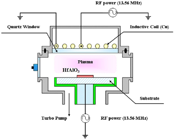
The HfAlO3 and SiO2 thin films were deposited on Si(100) wafers by atomic layer deposition (ALD) and thermal oxidation, respectively. The thickness of the HfAlO3 thin films was 50 nm and that of SiO2 was 10 nm. Before the deposition of the HfAlO3 thin films, a pre cleaning and oxidation step of the Si wafer is required in order to obtain good thermal interface compatibility between HfAlO3 thin film and the silicon substrate. The dry etching of the HfAlO3 thin films was performed using an inductively coupled plasma (ICP) system (Fig. 1) [5]. The gases used in the etching experiments include Cl2, BCl3, and Ar. The gas mixing ratio was fixed at BCl3 (4 sccm)/Ar (16 sccm). The etching conditions were as follows: an RF power of 500 W, a DC-bias voltage of -100 V, and a process pressure of 2 Pa. The etch rates were measured using a depth profiler (alpha step 500, KLA Tencor). The chemical state of the etched HfAlO3 surface was analyzed by XPS. The XPS spectra were collected using a VG Scientific ESCALAB 250 instrument equipped with an analytical chamber pumped to a base pressure of ~10-10 torr, a twin-anode X-ray source, and a spherical sector analyzer with multichannel detectors. For the analysis, the samples were mounted on stainless steel stubs using doublesided adhesive tape. The spectra were excited using Al Kα radiation (hv= 1,486.6 eV). All XPS data were corrected for sample charging during X-ray irradiation using adventitious hydrocarbon referencing(C 1s at 284.6 eV).
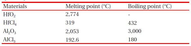
[Table 1.] Melting point and boiling point of the etch products at atmo-spheric pressure.

Melting point and boiling point of the etch products at atmo-spheric pressure.
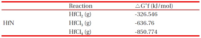
[Table 2.] Gibb’s free energy of volatile etch products in Hf-based material.

Gibb’s free energy of volatile etch products in Hf-based material.
For the characterization of the HfAlO3 thin films used in an ICP etching system, the plasma etching of the HfAlO3 thin films and the selectivity of HfAlO3 to SiO2 was investigated as a function of the Cl2/BCl3/Ar gas mixing ratio, an RF power, a DC-bias voltage and a process pressure.
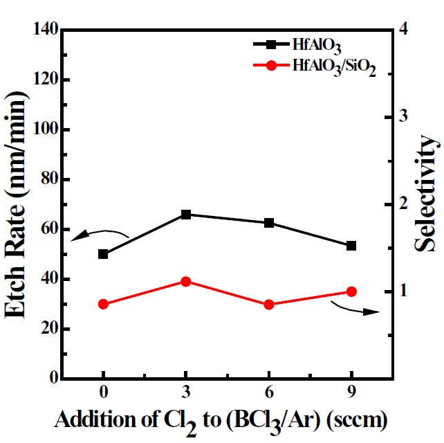
Figure 2 shows the etch rate of the HfAlO3 thin films and selectivity of the HfAlO3 to SiO2 as a function of the gas mixing ratio.The maximum etch rate of the HfAlO3 thin films were 66 nm/min on addition of Cl2 (3 sccm) to BCl3 (4 sccm)/Ar (16 sccm). The selectivity was maintained between 0.85 and 1.11. Table. 1 and 2 show the melting point, boiling point, and Gibb’s free energy, respectively.These data be explained by the fact by-products such as HfCl4 and AlCl3 were formed on the HfAlO3 thin films in the etching process [6]. When the Cl2 in BCl3 was increased from 0 sccm to 3 sccm (4 sccm)/Ar (16 sccm) plasma, the density of the Cl radical increased, which resulted in an increasing etch rate.However, the etch rate showed decreasing tendencies when the Cl2 content was increased from 3 sccm to 9 sccm in the BCl3 (4 sccm)/Ar (16 sccm) plasma. This result can be explained by the fact that the kinetic energy was decreased, which leads to fewer bonds breaking inside the HfAlO3 thin films under the influence of the Ar ion sputtering. Thus, the etch rate was decreased because of fewer reactions taking place on the surface, because of the low energy of the radical [7]. From these facts it is evident that the etching mechanism acting on theHfAlO3 thin film can be described as a physically-assisted chemical reaction in the Cl2/BCl3/Ar plasma.
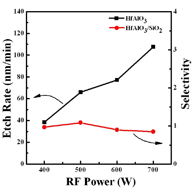
Figure 3 shows the etch rate of the HfAlO3 thin films and the selectivity of the HfAlO3 to SiO2 as a function of RF power. As the RF power applied to the ICP coil was raised from 400 to 700 W, the etch rates of the HfAlO3 thin films increased from 38.4 to 107.7 nm/min. As the RF power was increased, the etch rate of HfAlO3 also increased. Such behavior in response to increasing input power at all etch rates may be explained by the acceleration of both the physical and chemical etching pathways through the growth of volume densities and fluxes of ions and chlorine atoms [8].
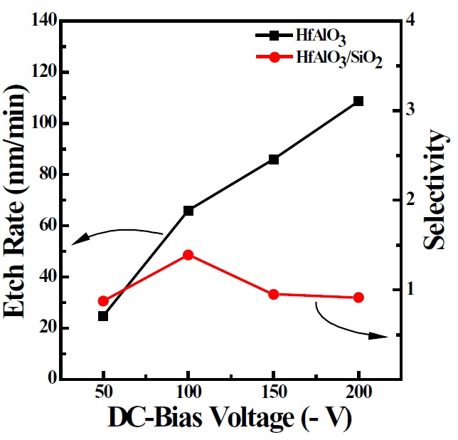
Figure 4 shows the etch rate of the HfAlO3 thin films and selectivity of HfAlO3 to SiO2 as a function of DC-bias voltage. As the DC-bias voltage is increased from 50 to 200 V, the etch rate of the HfAlO3 thin films increases from 24.8 to 108.6 nm/min. As the DC-bias voltage increases, the etch rate of the HfAlO3 increased. We can explain this result in terms of the increased electric field intensity caused by the increase in DC-bias voltage. An increased electric field intensity produces a higher ion bombardment energy [9]. Also, an increase in the etch rate can be related to the increase in the mean ion energy which generates increased sputtering yields for both the HfAlO3 thin films and the reaction products.
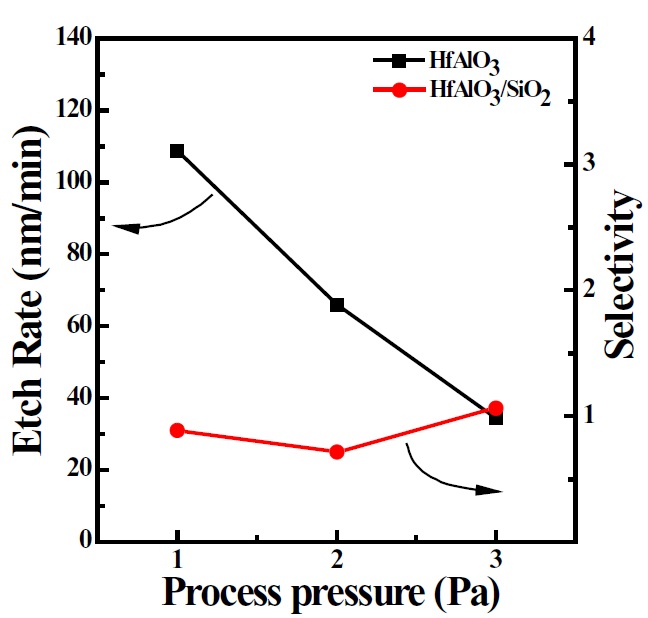
Figure 5 shows the etch rate of the HfAlO3 thin films and the selectivity of HfAlO3 to SiO2 as a function of process pressure. As the process pressure is increased from 1 to 3 Pa, a furthermore decrease in gas pressure up to 3 Pa results in a decrease in the HfAlO3 thin film etch rate in the range of 108.75-34.5 nm/min.With a decrease in process pressure, the average ion energy increases because of the longer mean-free-path. When the meanfree-path increases, the probability of collisions and charge transfer decrease in the substrate sheath region [10]. This can be explained by the fact that the increase in the etch rate at lowpressure is due to an increase in both the flux and energy of the bombarding ions, caused by the increased mean-free-path.
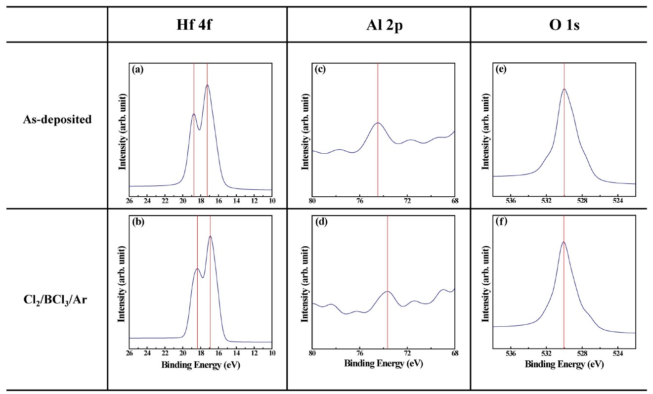
In order to analyze the chemical states for the HfAlO3 thin films, the HfAlO3 surface exposed to the Cl2 (3 sccm)/BCl3 (4 sccm)/Ar (16 sccm) plasma was investigated by XPS. The input plasma parameters were set to an RF power of 500 W, a DC-bias voltage of -100 V, a process pressure of 2 Pa and a substrate temperature of 40°C. Figures 6(a)-(f ) show the XPS narrow scan spectra of the HfAlO3. No boron or chlorine peaks were detected. This result implies that the boron and chlorine compounds are highly volatile ones such as boron-oxy-chloride (BOCl) or trichloroboroxin(BOCl)3 [11].
Figures 6(a) and (b) show the peaks of the Hf 4f XPS narrow scan spectra of the as-deposited and etched HfAlO3 thin films in Cl2/BCl3/Ar. There are two strong peaks at 18.8 eV and 17.1 eV from the as-deposited sample, which correspond to Hf 4f5/2 and Hf 4f7/2, respectively. These peaks moved toward a lower binding energy and their maximum deviation was about Δ 0.3 eV when the HfAlO3 thin films were exposed to the Cl2/BCl3/Ar plasma.This chemical shift indicates that there are chemical reactions between the Hf and Cl radicals and the resulting etch byproducts remain on the surface. Figures 6(c) and (d) show the peaks of the Al 2p XPS narrow scan spectra of the as-deposited and etched HfAlO3 thin films in Cl2/BCl3/Ar. There are peaks at 74.5 eV and 73.7 eV from the as-deposited sample and the sample etched in Cl2/BCl3/Ar, respectively. These peaks moved toward a lower binding energy and the maximum deviation was about Δ 0.8 eV. Compared with the as-deposited film, the Al peak intensity decreased when the HfAlO3 thin films were exposed to the Cl2/BCl3/Ar plasma. This result means that Al atoms were removed from the HfAlO3 thin films. The surface of the HfAlO3 thin film reacts with the Cl radicals dissociated in the plasma, producing chloride compounds such as AlCl3. Figures 6(e) and (f ) show the peaks of the O 1s XPS narrow scan spectra of the as-deposited and etched HfAlO3 thin films in Cl2/BCl3/Ar. There are strong peaks at 530 eV from the as-deposited sample and sample etched in Cl2/BCl3/Ar, respectively. There are no changes of intensity and binding energy for the O 1s peaks. This result means that the O atoms did not react.
Therefore, the XPS data give clear confirmation that the surface of the etched HfAlO3 film is covered by low volatility etch products such as Hf-Cl4 and Al-Cl3. In this situation, the ionstimulated desorption of the reaction products can be assumed to be the limiting stage for the etching process in the Cl2 and BCl3 rich plasmas whilst the etch rate is expected to be rather sensitive to the factors which are influenced by the ion bombardment.
In this study, the etching trend of the HfAlO3 thin films was investigated as functions of the Cl2/BCl3/Ar gas mixing ratio, the RF power, the DC-bias voltage and the process pressure, using ICP.The maximum etch rate of the HfAlO3 thin films was 108.7 nm/min and the selectivity of HfAlO3 to SiO2 was 1.11 at Cl2 (3 ccm)/BCl3 (4 sccm)/Ar (16 sccm). When the Cl2 concentration was increased beyond 3 sccm, the etch rate of the HfAlO3 thin film decreased, because higher concentrations of Cl2 in the plasma decreased the physical effect. The HfAlO3 etch rate increased linearly with increasing RF power and DC-bias voltage. However,we found that the maximum etch rate trend did not follow this trend. This result can be explained by the characteristics of the inner plasma, which is easily affected by the input parameters.The narrow scan of the XPS measurement showed that the binding energies of the Hf 4f7/2, Hf 4f5/2, and Al 2p peaks were shifted toward lower binding energies after the exposure of the films to the Cl2/BCl3/Ar plasma caused by the chemical reaction or intensity changes. From the results of the etch rate and analyses of XPS for HfAlO3, the most probable determinant of the maximum etch rate can be defined as an ion-assisted chemical etching in Cl2/BCl3/Ar plasma.