Over the last decade, ferroelectric thin films have been widely investigated for nonvolatile memory applications [1-12]. Among ferroelectric materials, lead-zirconate-titanate (PZT) has been considered to be the most promising candidate for memory applications [1-3]. However, serious limitations have been encountered, such as the loss of Pb, fatigue, and space charges between the ferroelectric thin film and the electrode [2,3]. To address these problems, various ferroelectric and electrode materials, such as bismuth-based (SrBi2Ta2O9), barium-based (BaTiO3), RuO2, and La0.5Sr0.5CoO3, have been extensively studied [4-6]. But these materials exhibited low polarization and high resistivity. In contrast to the aforementioned ferroelectric materials, antiferroelectric materials exhibited were 180° domain switching behavior. One hundred and eighty degree domain switching possesses better fatigue properties in comparison to 90° domain switching due to its smaller internal stresses [7,8]. Also, through a doping donor and appropriate electrode materials, antiferroelectric materials may encompass ferroelectric properties [8,9]. In this study, in order to improve the ferroelectric property and crystallinity of the antiferroelectric material, Sn and Nb were doped in PZT materials. The PNZST thin films were deposited on (La0.5Sr0.5) CoO3/Pt/Ti bottom electrode by a radio frequency (RF) magnetron sputtering method and were annealed by the rapid thermal annealing (RTA) method. The microstructural characteristics and electrical properties of the PNZST thin films were investigated under varying RF magnetron sputtering parameters and annealing conditions.
The substrates used in this experiment were (100)-oriented p-type Si wafers with a polished surface oxidized in a wet O2 atmosphere. The thickness of the SiO2 layer was approximately 600 nm. The LSCO/Pt/Ti electrode was prepared on SiO2/Si substrate by a RF magnetron sputtering method. The Pt (150 nm) thin films were used as a bottom electrode, and Ti (20 nm) thin films were used to increase adhesion. The LSCO thin films were deposited on Pt/Ti/SiO2/Si at 400℃ and annealed at 700℃ in O2 ambient to serve as a tolerable barrier against Pb diffusion [10]. A LSCO target of 2 inch diameter was sputtered in an Ar and O2 ambience with the gas pressure of 10 mtorr at the power of 50
[Table 1.] Sputtering and annealing conditions of PNZST thin films.
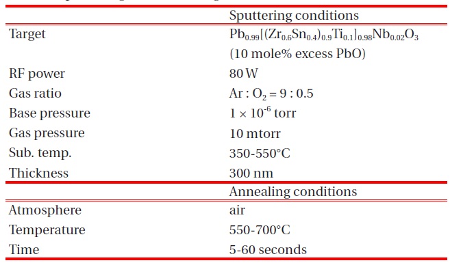
Sputtering and annealing conditions of PNZST thin films.
W. The thickness of the LSCO thin films was about 100 nm. Ferroelectric PNZST thin films were deposited at various conditions by a RF magnetron sputtering method. A PNZST target of 2 inch diameter was prepared by sintering at 1,150℃ for 3 hours [10]. An excess of 10 mole% PbO powder was added to the target materials to compensate for the loss of Pb during deposition and post-annealing processes.
To improve crystallinity of the as-deposited PNZST thin films, the thin films were annealed at various conditions. The sputtering and annealing conditions of the thin films are summarized in Table 1. The Pt top electrodes with an area of 0.25 mm2 were deposited by RF magnetron sputtering method and were defined by the lift-off process. The thickness of the thin films was measured by a surface profiler. The structural properties of the thin films were analyzed by X-ray diffraction using Cu-Kα radiation. The measurements of electrical properties were carried out using an impedance analyzer and a ferroelectric tester.
The crystallinity of PZT-based thin films deposited by a RF magnetron sputtering method depend strongly on substrate temperature, bottom electrode materials, film thickness, and
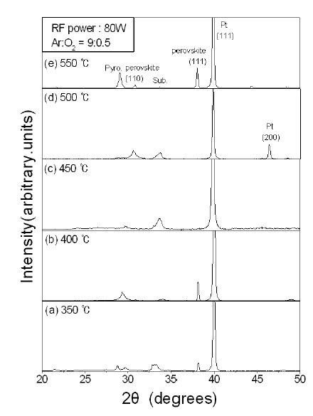
annealing conditions [11]. Figure 1 shows the X-ray diffraction curves of PNZST thin films deposited at different substrate temperatures, ranging from 350℃ to 550℃. For the PNZST thin film deposited at 350°C, the dominant peak observed at 2θ = 40° was a result of the (111)-oriented Pt, and (111)-oriented perovskite phase peak appeared at 2θ = 38.1°. However, the pyrochlore phase peak was also observed at 2θ = 29°. For the PNZST thin film deposited at 400℃, the intensity of the (111)-oriented perovskite phase peak increased. However, the intensity of pyrochlore phase peak also increased, as shown in Fig. 1(b). As the substrate temperature increased from 400℃ to 450℃, the intensity of the pyrochlore phase peak decreased. When the substrate temperature increased to 500℃, the (110)-oriented perovskite peak began to appear at 2θ = 30.9° and pyrochlore phase peak disappeared, as shown in Fig. 1(d). But, the intensity of the perovskite phase
was not high. For the PNZST thin films deposited over 500℃, the intensity of the (110)-priented perovskite phase peak decreased, and the (111)-oriented perovskite phase peak coexisted with pyrochlore phase, as shown in Fig. 1(e). These results show that a suitable substrate temperature promotes crystallinity of the perovskite phase.
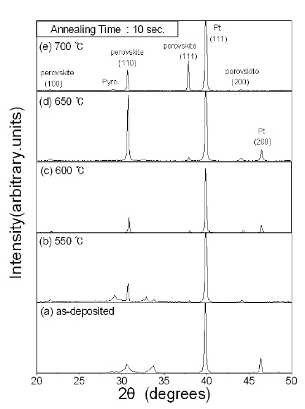
PNZST thin films were deposited at the substrate temperature of 500℃, and then annealed at different temperatures for 10 seconds in air. The X-ray diffraction curves of the PNZST are shown in Fig. 2. The (110)-oriented PNZST main perovskite peak existed in all cases, and its intensity was much stronger than any other PNZST peaks except for the Pt peak; thus indicating that the annealing process improves crystallinity of the (110)-oriented PNZST perovskite phase and depresses crystallinity of the pyrochlore phase. According to the increase of the annealing temperature, the intensity of the (110)-oriented perovskite peak increased at 2θ = 30.9°, and its magnitude was the largest at 650℃, as shown in Figs. 2(b)-(d). In Fig. 2(e), when the annealing temperature increased to 700℃, the intensity of the (111)-oriented PNZST perovskite peak increased, while the other peaks had negligible
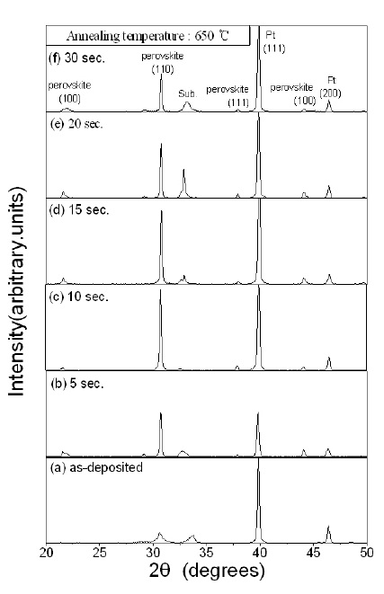
changes. This reveals that the annealing temperature has a greater and more significant effect on the crystallinity of thin films rather than the substrate temperature [12]. Perovskite-type PNZST thin films can be obtained by RF magnetron sputtering provided that the films are annealed at high temperatures. Hence, the annealing process benefits the formation of the crystalline perovskite phase. Figure 3 shows the X-ray diffraction curves of the PNZST thin films deposited at the substrate temperature of 500℃ and then annealed in air at 650℃ for various times. For the PNZST thin film annealed at 650℃ for 10 seconds, the intensity of the (100)-oriented perovskite peak was the largest.
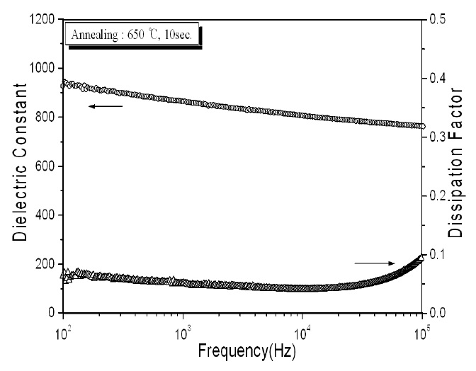
Figure 4 shows the dielectric constant and the dissipation factor of the PNZST thin films as a function of frequency. In this measurement, the PNZST thin films were deposited at the substrate temperature of 500℃, and annealed at 650℃ for 10 seconds in air. The amplitude of the ramp voltage was 10 mV and the frequency ranged from 100 Hz to 100 kHz. The observed values of the dielectric constant and dissipation factor at 1 kHz were approximately 861 and 0.05, respectively. The decrease in the dielectric constant may be attributed to the effects of the interfacial polarization at the contacts and Maxwell-Wagner polarization of grain boundaries [13].
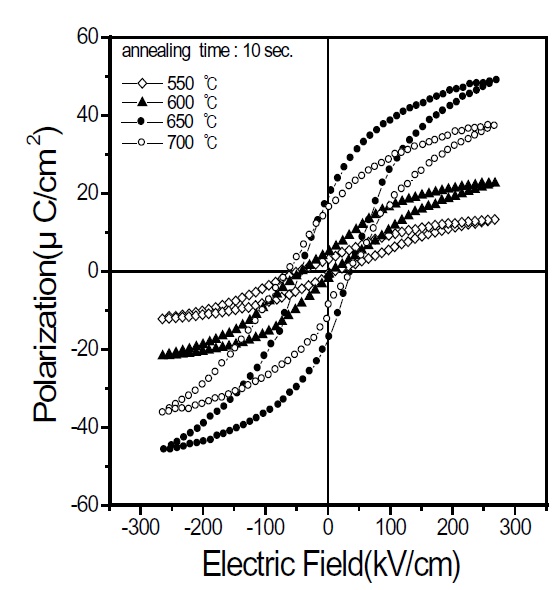
The ferroelectric properties were investigated by measuring the polarization hysteresis loop, as shown in Fig. 5. The PNZST thin films were deposited at the substrate temperature of 500℃, and annealed at different temperatures for 10 seconds in air. From Fig. 5, the remanent polarization and coercive field of the PNZST thin film annealed at 650℃ were approximately 20 uC/ cm2 and 50 kV/cm, respectively. These values were superior to those obtained for sol-gel derived PNZST films [9], and exhibited a low coercive field. In our results, it is thought that a low coercive field is due to the decrease of the space charge layer inside each ferroelectric domain by doping Sn and Nb in PZT [12]. In general, the slightly lower Pr and higher Ec may be associated with the smaller grain size in thinner films. The increase in Ec with decreasing film thickness is attributed to stresses induced in the films [14], and similar effects are also observed for bulk ceramics. This effect is due to the space charge layer inside each ferroelectric domain [15].
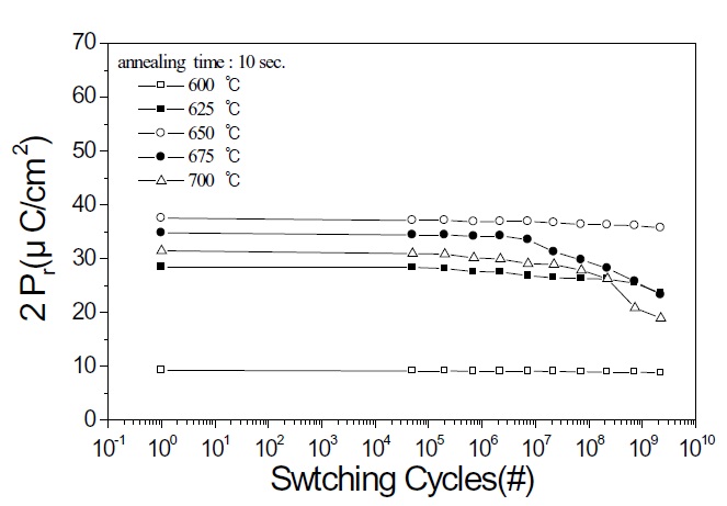
Figure 6 shows fatigue characteristics of the PNZST capacitor. In this measurement, the amplitude of the applied bipolar pulse stress was 167 kV/cm. For the PNZST thin film deposited at 500℃ and annealed at 650℃ for 10 seconds in air, the reduction of 2Pr after 2.2 × 10⁹ switching cycles is less than 10%. This result is also observed in the sol-gel derived PZT capacitor with a LSCO bottom electrode [6], and it is thought that the PNZST thin film matches the bottom electrode in the interface.
In summary, Pb0.99[(Zr0.6Sn0.4)0.9Ti0.1]0.98Nb0.02O3 ferroelectric thin films have been deposited by RF magnetron sputtering. After annealing, the thin films were completely crystallized into the perovskite phase. When the thin films were deposited at the substrate temperature of 500℃, and were annealed at 650℃ for 10 seconds in air, these films exhibited good crystallinity and ferroelectric properties. Typical values for the remanent polarization and the coercive field are about 20 uC/cm2 and 50 kV/cm, respectively.