Recently, there has been considerable interest in the use of Sn-doped In2O3 (ITO) films deposited on polymer substrates for transparent electrodes in flexible display devices [1,2] due to the fact that they are lighter and more flexible than ITO films deposited on glass substrates.
However, polymer substrates are inherently sensitive to moisture and oxygen and the rough surface of polymers may deteriorate the electrical and optical performance of flexible displays. Thus, in order to overcome these problems, transparent diffusion barrier films have been extensively researched to provide smooth surfaces, and may also reduce the diffusion of water vapor and oxygen into displays deposited on polymer substrates [3,4].
In this study, thin ITO films were deposited by radio frequency (RF) magnetron sputtering on glass substrates with and without a TiO2 buffer layer; then, the effect of TiO2 layers on the optical, electrical and structural properties of the ITO films were investigated using X-ray diffraction (XRD), atomic force microscopy (AFM), Hall effect measurements, and UV-visible spectrometry. Also, the influence of the TiO2 buffer layer on the work function of ITO films was evaluated using UV photoelectron spectroscopy (UPS, KBSI Jeonju Center) to evaluate ITO/TiO2 films as transparent anode electrodes for organic light emitting diode (OLED) applications.
ITO and TiO2 thin films were deposited on glass substrates without intentional substrate heating using an RF (13.56 MHz) magnetron sputter equipped with two cathodes. The sintered In2O3 (95%)-SnO2 (5%) and pure TiO2 targets were both 3 inches in diameter and 0.25 inches thick.
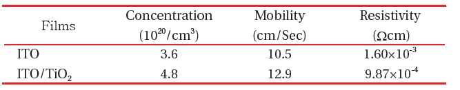
Prior to deposition, the chamber was evacuated to a pressure of 1.3×10⁻⁴ Pa and then ITO Sputtering was performed in an argon (Ar) and oxygen (O2) gas mixture. For all depositions, the distance between the target and substrate was constant at 6 cm and the substrate rotation speed was also set to 8 rpm. The ITO/TiO2 bi-layered films were obtained by continuously depositing each film layer without exposure of the films to the atmosphere. The substrate temperature was monitored using a K-type thermocouple in contact with the substrate and the substrate temperature increased to 70℃ during deposition. Table 1 depicts the main parameters used for deposition.
High resolution XRD (X’pert Pro MRD, Philips) at the Korea Basic Science Institute (KBSI, Daegu center) was used to observe the thin film crystallinity and the root mean square (RMS) roughness investigation was performed by means of an AFM (XE-100, Park system) on 2×2 Ωm2 sample areas under ambient conditions. Optical transmittance in the visible wavelength region was observed with a UV-Vis. spectrophotometer (Cary 100 Cone, Varian). The glass substrates showed 92% optical transmittance in the visible wavelength range. The thickness of the films was measured using a surface profilometer (Dektak 3D, Veeco), and the electrical properties of carrier concentration and mobility, were derived from Hall effect measurements employing the van der Pauw geometry (HMS-3000, Ecopia) using a permanent magnet of 0.5 T. The performance of ITO and ITO/TiO2 films as transparent conducting films were compared, using a figure of merit [5]. In addition, to consider the influence of a TiO2 buffer layer on the work function of ITO films, work functions of the films were evaluated using UPS analysis.
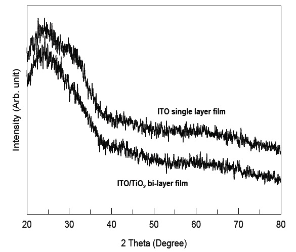
Figure 1 shows the XRD patterns of the as-deposited ITO films and ITO/TiO2 bi-layer films. As shown in Fig. 1, neither film showed any diffraction peaks of In2O3 or SnO2. Shigesato et al. [6] investigated the growth mode of ITO on a glass substrate over the temperature range of 100~400℃ and found that ITO films formed at substrate temperatures below 200℃ had an amorphous structure. The amorphous XRD pattern observed in Fig. 1 is consistent with previously reported papers [6].
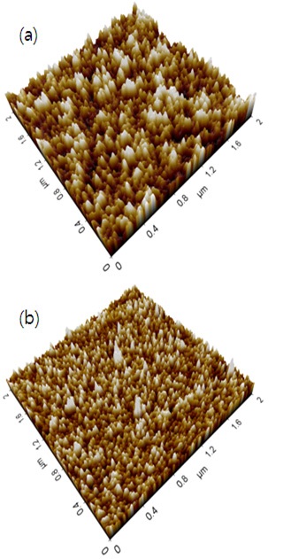
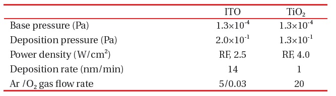
Surface roughness of ITO films is an important factor in determining the quality of the OLED device. Since in OLED devices, the distance between anode and cathode is only several hundred nanometers, it is critical that the ITO film’s surface be smooth to reduce current leakage pathways caused by irregular surface protrusions [7]. Therefore, it is critical to prepare anode ITO films that have atomically smooth surfaces to eliminate the current leakage pathways caused by rough surfaces. Figure 2 shows AFM images of ITO films prepared on bare glass substrates and on TiO2 deposited on glass substrate. As shown in Fig. 2, all the films show a relatively smooth surface morphology. The root mean square (RMS) roughness of the ITO film (1.7 nm) is larger than that of the ITO/TiO2 film (1.2 nm). From the AFM images, one can conclude that TiO2 buffer layers may enhance the flatness of the ITO/TiO2 films. In a previous study, J. Park reported that a Ni interlayer in ITO/Ni/ITO multilayer films also promotes the flatness of the upper ITO films [8].
Table 2 shows the influence of the TiO2 buffer layer on the electrical properties of the films. The ITO/TiO2 films have a lower resistivity of 9.87×10⁻⁴ Ωcm than that of the ITO single layer film due to increases in both carrier concentration and mobility. Similarly, Herrero et al. [4] prepared ITO/ZnO films on glass substrates, and the resistivity of the films was about 1.2×10⁻³ Ωcm. Thus, TiO2 is a proper buffer layer for the deposition of ITO films.
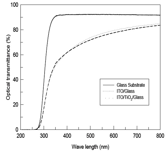
Figure 3 shows the optical transmittance for ITO and ITO/TiO2 films. For the ITO single layer film, the average transmittance in the visible range is about 75.9% and the transmittance of ITO/TiO2 film is about 76.1%.
Table 3 provides a comparison of the optical and electrical properties of the films. The ITO/TiO2 films had a lower sheet resistance than that of the ITO single layer films. The figure of merit
[Table 1.] Deposition conditions of ITO and TiO2 thin films.
Deposition conditions of ITO and TiO2 thin films.
[Table 2.] Comparison of the electrical properties of the films.
Comparison of the electrical properties of the films.
[Table 3.] Comparison of the figure of merit (FOM, Ω-1).
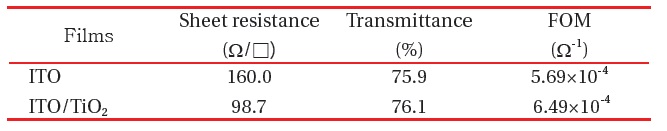
Comparison of the figure of merit (FOM, Ω-1).
(FOM) is an important index for evaluating the performance of transparent conducting oxide (TCO) films. The FOM is defined as FOM= T10/Rs, where T is the optical transmittance and Rs is the sheet resistance [9].
Although the optical transmittance of ITO films deteriorated with the TiO2 buffer layer, ITO/TiO2 films have one order lower resistivity than that of the ITO single layer films, as shown in Table 2. Thus, the FOM reached a maximum of 6.49×10⁻⁴ Ω-1 for the ITO/TiO2 films, which is greater than the 5.69×10⁻⁴ Ω-1 FOM for the ITO single layer films prepared in this study. Since the higher FOM value indicates better quality TCO films, it is supposed that the ITO film with a 5-nm-thick TiO2 buffer layer will likely perform better in TCO applications than ITO single layer films.
The high work function of ITO films, which is close to the value of the highest occupied molecular orbital (HOMO) of the organic layer, allows hole injection from ITO to the organic
layer of OLED, which results in a decrease in the turn-on voltage of the OLED. However, the work function of conventional ITO films is lower than the HOMO of the organic layer of OLEDs. Thus, several techniques have been developed to increase the work function of ITO [10,11].
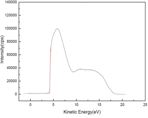
Figure 4 shows the kinetic energy cut-off spectra obtained from the ITO/TiO2 films. This allowed the determination of the work function values directly from the spectra by fitting straight lines into their kinetic energy cut-off and determining the intersect with the baseline of the spectra. The work function of pure ITO films is known to be 3.9 eV [12].
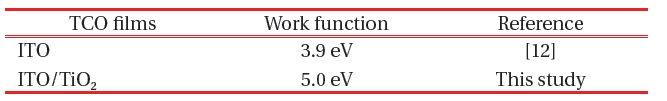
Table 4 shows a comparison of the work function of ITO and ITO/TiO2 films. The ITO/TiO2 films show a higher work function
[Table 4.] Comparison of the work function of the films.

Comparison of the work function of the films.
of 5.0 eV. Thus, adding a TiO2 buffer layer is one of the useful methods to increase the work function of ITO films.
Both ITO single layer and ITO/TiO2 bi-layered films were prepared by RF magnetron sputtering on glass substrates. The optical and electrical properties of the ITO films were dependent on the TiO2 buffer layer.
From AFM observations, it is apparent that TiO2 buffer films enhance the flatness of the ITO/TiO2 films. The figure of merit for the ITO 100 nm/TiO2 5 nm films reached a maximum value of 6.4×10⁻⁴ Ω-1, which was greater than that of the ITO single layer films.