Single wall carbon nanotubes (SWCNTs) continue to attract extensive interest because of their unique electronic, structural, and mechnical properties [1,2]. These unique and superb properties make SWCNTs good candidates for application in various fields, such as nanoelectronics [3], information displays [4], energy storage mediums [5], atomic force microscopy (AFM) [6], and so on. These application fields prefer isolated SWCNTs to bundled ones since the isolated SWCNT has several advantages over its counterpart. For instance, the narrow diameter of an isolated SWCNT is very useful as a field emission tip and AFM probe. Its large specific surface area is extremely important in vehicle energy storage, and sensor applications. In particular, isolated SWCNTs are specifically requested for SWCNTbased nano-electronics because bundled SWCNTs contain both semiconducting and metallic nanotubes, which alters their properties and function.
To utilize SWCNTs in these applications, many researchers have tried to synthesize isolated nanotubes using various techniques, such as arc-discharge [7], laser vaporization [8], and chemical vapor deposition (CVD) [9]. However, due to the very strong van der Waals force between individual nanotubes, most SWCNTs produced so far are in a bundled state, which are not useful for practical applications. For this reason, there have been a number of studies on the nano-dispersion (de-bundling) of SWCNTs as a second-best alternative to producing them singly [10-12].
Among the application fields mentioned above, one of the most intriguing applications is the use of carbon nanotubes in nano-electronic devices, since the feature size of current electronic devices has already reached the minimum state for practical fabrication. Producing a nanosized device using isolated SWCNTs is expected to open the next generation of the semiconducting electronics industry. Such nano-electronics would require isolated SWCNTs doped with n-type or p-type dopants. The synthesis of isolated SWCNTs has been reported on oxidized silicon [13] and AFM probe [14] by CVD using ethylene gas as a carbon source.
However, it is not straightforward to dope SWCNTs when they are produced by hydrocarbon gas sources, such as ethylene.
In the present study, we synthesized isolated SWCNTs on quartz and silicon oxide substrates by the CVD method using liquid state xylene as a carbon source. This liquid precusor-based growth makes it possible to produce doped isolated SWCNTs by adding soluble dopants into the precursor. A preliminary study on the synthesis of nitrogen-doped isolated SWCNTs was also carried out to demonstrate the potential of this doping method.
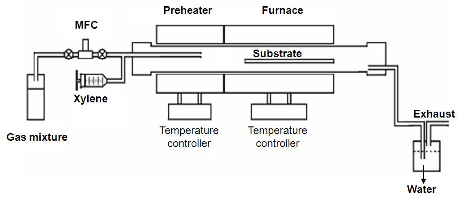
Isolated SWCNTs were grown on quartz and thermally oxidized silicon substrates by CVD using xylene as a carbon source. Iron (III) nitrate nonahydrate powder was dissolved in 2-propanol. The substrates were dipped in this solution for 10 s and then immersed in hexane for 1 s. The substrates were loaded in a quartz tube reactor (1.5'' in dia.) and then heated to 750℃ with a heating rate of 24℃/min. While the temperature was being increased, argon and hydrogen gases were flowed with flow rates of 600 sccm and 400 sccm, respectively. As soon as the temperature was stabilized at 750℃, xylene was injected into the quartz reactor for 30 min, then the furnace was cooled down under argon atmosphere. Fig. 1 shows the schematic diagram of the CVD used in this study. We used a two-step CVD that is composed of low and high temperature zones. Xylene is injected into the low temperature zone where the temperature is 200℃. Injected xylene is vaporized in this zone, and then carried to the high temperature zone (750℃) by the argon and hydrogen gases.
To investigate the morphologies of the carbon nanotubes grown on the substrates, they were scanned by AFM. Transmission electron microscopy (TEM) was used to measure the diameters of the SWCNTs and to confirm they were isolated singlewalled structures. For TEM measurements, we grew SWCNTs directly on silicon oxide-coated TEM grids using the same process of isolated SWCNT growth. A Raman microscope with a focusing area of 1 μm in diameter was also used to analyze the SWCNTs. The excitation wavelength of the laser was 785 nm, corresponding to Elaser = 1.58 eV. Based on the Raman spectra, we could determine diameters, chiralities, and the metallic/semiconducting nature of isolated SWCNTs.
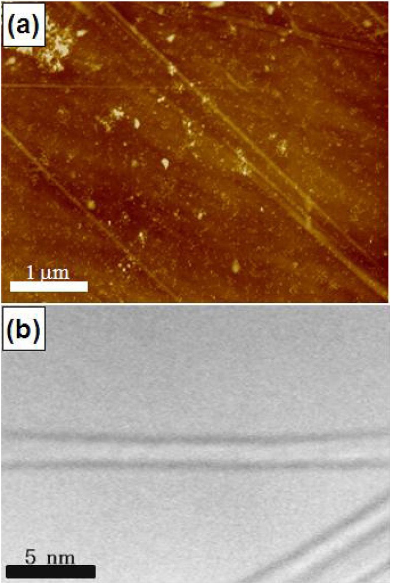
Fig. 2a is an AFM image showing isolated SWCNTs synthesized on a quartz substrate. It can clearly be seen that isolated SWCNTs have been successfully synthesized by this process. The SWCNTs have a very straight morphology, indicating high crystallinity. The height profile observed during AFM measurement revealed that the diameters of the isolated SWCNTs ranged
from 1 nm to 2 nm. Fig. 2b shows a TEM image confirming the isolated single-walled structure of the synthesized nanotubes. The diameters observed in the TEM image ranged from 1.2 to 1.7 nm, which is in good agreement with the AFM observations. It is believed that the variation of nanotube diameter originates from the different sizes of catalyst particles. In order to grow the isolated SWCNTs seen in Fig. 2a, 3 mg of iron (III) nitrate nonahydrate powder was dissolved in 20 mL of 2-propanol so as to form catalytic iron particles on the substrate. It was found that the density of isolated SWCNTs could be controlled by varying the concentration of iron (III) nitrate nonahydrate/2-propanol solution. We observed a noticeable decrease in the number of SWCNTs when the amount of 2-propanol was increased to 40 ml. The isolated SWCNTs could also be synthesized on thermally oxidized silicon substrate, as verified in the following Raman spectra (Fig. 3). However, we could not achieve the growth of SWCNTs on bare silicon substrate. We speculate that the polished surface of the bare silicon substrate is too smooth to nucleate SWCNTs.
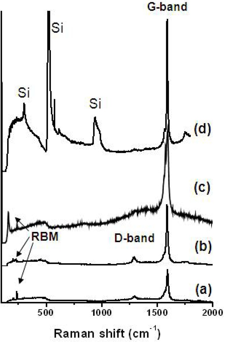
The Raman spectra of isolated SWCNTs grown on quartz and thermally oxidized silicon substrates are presented in Fig. 3. The spectra were taken with a focusing diameter of 1 μm using a laser with excitation wavelength of 785 nm, corresponding to 1.58 eV. Figs. 3a-c are the Raman spectra obtained at three different positions on the quartz substrate, and Fig. 3d shows the spectrum of SWCNTs synthesized on thermally oxidized silicon substrate. Tangential G-band peaks around 1590 cm-1 were detected with shoulder peaks in the low wavenumber region in all spectra, indicating good formation of SWCNTs [15]. The intensity of the
disorder induced D-band around 1300 cm-1 is small enough to be neglected, meaning that amorphous carbon particles and defects such as pentagons and heptagons in the nanotube structures were hardly formed during the growth process. Radial breathing mode (RBM) peaks are seen in the three spectra obtained from the quartz substrates, although their frequencies are different from each other. The different wavenumbers of the RBM peaks originate from the difference in diameters of the isolated SWCNTs. Although an RBM peak is not seen in the sample grown on the oxidized silicon substrate, shown in Fig. 3d, we believe that there are RBM peaks buried in the broad (100 to 500 cm-1) silicon peak, since the second order Raman peak at around 1750 cm-1 in Fig. 3d is due to the combination of RBM and tangential mode [16].
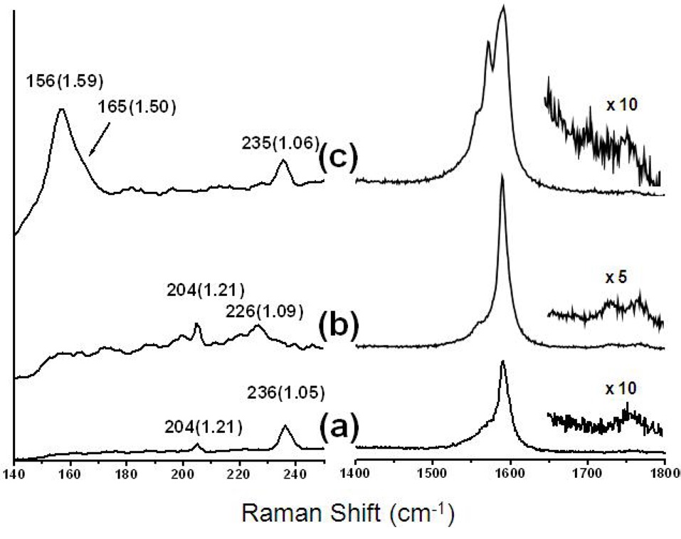
Fig. 4 shows three Raman spectra in the RBM region and the G-band taken from three different regions on a quartz substrate. Each spectrum in the figure has at least two RBM modes, which means that there were at least two isolated SWCNTs in the laser focusing area of 1 μm diameter. This could be expected from the AFM image seen in Fig. 2. The RBM peak frequency,
The chirality (
carmetallic and semiconducting nanotubes and their calculated
Note that Fig. 4 represents the different morphologies of the tangential G-band peaks located at around 1590 cm-1. The G-band is an intrinsic feature of all sp2 carbon materials since it is derived from the Raman-allowed optical mode
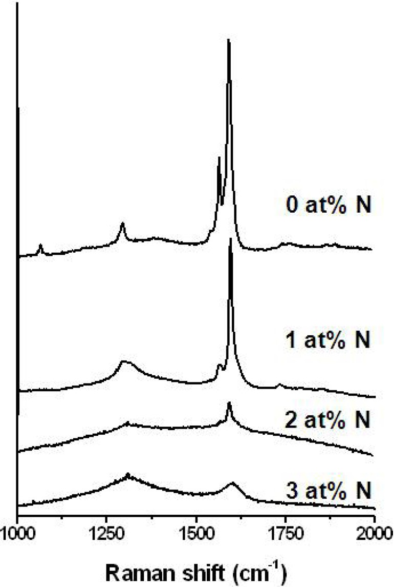
The advantage of our synthesis technique is that the growth of doped isolated SWCNTs was easily achieved by using liquid precursor (xylene) as the carbon source. Specifically, nitrogendoped (n-type) SWCNTs could be achieved using acetonitrile that is soluble into xylene. A preliminary study on the synthesis of nitrogen doped SWCNTs was carried out, and its Raman spectra are shown in Fig. 5. The amount of nitrogen to carbon in the precursor ranged from 0 to 3 at%. With increasing nitrogen atomic content, the intensity of the tangential G-band peak decreased, and finally, at 3 at%, the G-band peak, a characteristic feature of single walled SWCNTs, disappeared. In addition, the ratio of the intensity of G-band to D-band (IG/ID) decreased dramatically at a nitrogen content over 2 at%, which implies that the incorporation of nitrogen atoms induces significant disorder in the graphene sheet of the isolated SWCNTs. This is also comfirmed by the appearence of D'-band peaks located at around 1610 cm-1 (shoulder peaks at the high wavenumber region of G-band) in the spectra of 1 and 2 at% samples.
Isolated SWCNTs were successfully grown on quartz and oxidized silicon substrates using xylene as the carbon source. The diameters of the SWCNTs ranged from 1 to 2 nm, as measured by AFM, TEM, and Raman analyses, and their chiralities were predicted based on the energy of the laser and their diameter. Analyses of the RBM and tangential G-band peaks showed that both metallic and semiconducting SWCNTs were being synthesized on a substrate. Nitrogen-doped isolated SWCNTs were also synthesized by adding acetonitrile to xylene. The crystallinity of the doped SWCNTs was found to decrease as the nitrogen content increased.