Recently, there is a concentrated research effort on the applications using the metamaterial-based transmission lines (MTM-TLs)-or right/left-handed transmission line (RLH-TL)-such as leaky-wave antennas, couplers, phase shifters, etc. [1]. A zeroth-order resonant (ZOR) antenna is one of the important applications of the MTM because it can be designed to be very compact. However, a disadvantage of the ZOR antenna is its narrow operating bandwidth. On the other hand, recent antennas for present day wireless communication require a compact size and wideband property for the transfer of a huge amount of information. In [2], a wideband epsilon negative (ENG) ZOR antenna using a mushroom structure was presented at an operating frequency of 9.2 GHz. It has relatively wide bandwidth of about 20%. The mushroom structures cannot be used for commercial services in the frequency range between 700 MHz to 3 GHz since it has very small shunt inductance. In [3], a miniaturized ENG ZOR patch antenna with an improved bandwidth was proposed. The miniaturization and broad bandwidth of the antenna is achieved by using a meandered via and a high permeability substrate. A tunable internal antenna with an ENG ZOR property has been presented for the digital video broadcasting-handheld service with a tuning range from 474 to 702 MHz [4]. The size of the antenna is very compact, but its voltage standing wave ratio (VSWR) is large (about 2 to 4.5). In this letter, an open-terminated tunable double-negative (DNG) ZOR antenna at 2.3 to 3.1 GHz with a very compact size and small VSWR is proposed using a varactor. The required shunt inductance is realized using a stub and varactor. Its performances are evaluated in terms of dispersion curves, reflection coefficients, and radiation patterns.
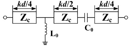
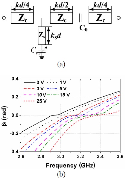
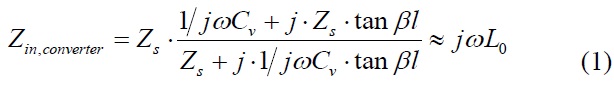
Fig. 1 shows the equivalent circuit of an asymmetric 1-D MTM-TL unit cell. The unit cell has been modified from a symmetric shape [5] in order to facilitate open (or short) termination for resonant antenna applications. The unit cell of the MTM line usually consists of a series capacitor with C0, shunt inductor with L0, and conventional transmission line (RH-TL) section with an electrical length of kd. The RH-TL is characterized by the series inductance Ld and shunt capacitance Cd. The ZOR has been extensively analyzed and its design equations have been provided in [6]. Fig. 2(a) and (b) show the equivalent circuit of the tunable DNG MTM-TL unit cell and its dispersion curves for different values of the bias voltages VBias. The shunt inductance L0 is replaced with a variable capacitor and a section of stub to provide a tuning operation of the MTM-TL. The characteristic impedance Zs of the stub has been chosen to be 100 Ω (line width=1.3 mm) to ensure that the stub line width is adequate for the connection to the main line. Its electrical length has been optimized to be 58° at 3 GHz for a wide tuning range and compact design. The SMV1405 (Skyworks Solution Inc.) plastic packaged abrupt junction varactor diode has been selected to control the Cv values. The recommended capacitance range of the varactor is from 2.67 to 0.63 pF with the necessary reverse bias voltages from 0 to 30 V. The used varactor model in the simulations is the lumped series RC circuit with R=0.8 Ω and recommended capacitances. We restrict the use of the Cv values from 2.67 pF (about 0 V) to 0.7 pF (about 25 V). For this range, the tuned L0 which is determined by (1) is from 5.64 nH to about 2 nH at 3 GHz.
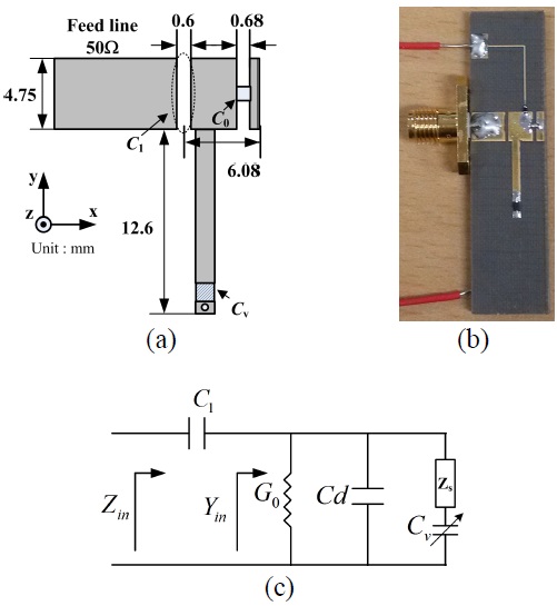
Using [5], the determined design value of C0 is 2 pF at 3 GHz. In Fig. 2(b), the dispersion curves for βd are shown to cross zero between 2.9 and 3.4 GHz. The name of the ZOR antenna comes from the property of βd=0. Due to the tuning of L0, the line becomes somewhat unbalanced. For the antenna applications with one unit cell, that effect is not serious, or even negligible, in the used frequency band. Fig. 3(a) and (b) show the proposed structure of the open-terminated tunable DNG ZOR antenna with impedance convertor, designed on a microstrip line and fabricated antenna, respectively. Its equivalent circuit can be simplified as shown in Fig. 3(c). The antenna substrate is a Tefron (εr=2.2, height= 1.6 mm). The ground plane size is 12 mm×60 mm. The antenna size is very compact (6 mm×17.4 mm, 0.05 λ0×0.2 λ0). The antenna consists of the RH line with electrical length kd of 30°, a series capacitor with C0, impedance convertor, and coupling capacitor C1. With the use of the coupling capacitor, the resonant frequency of the antenna shifts somewhat downward [6]. The DC bias feeding line in Fig. 3(b) is designed to effectively protect the radio frequency (RF) line from the bias line at resonant frequencies with the open-ended TL with 200 Ω(the thinnest possible), and a resistor with 5 MΩ. It means that the bias line seems to be an open circuit at resonant frequencies. The spacing between the RF line and the bias source point has been chosen to be 10 mm for reduced coupling between the line and RF line. It means that the radiation patterns are not influenced by the bias line.
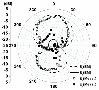
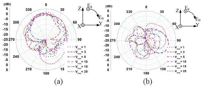
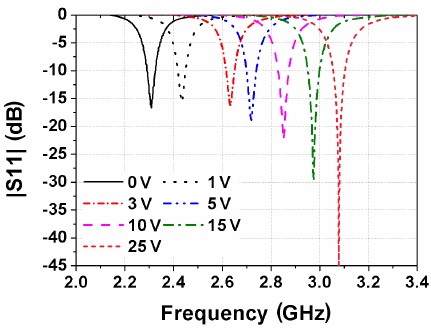
The |S11|’s of the antenna versus frequency for different bias voltages are shown in Fig. 4. The resonant frequency of the antenna sweeps between 3.08 and 2.31 GHz by changing the capacitance of the varactor using the DC bias voltage from 0 to 25 V. The tunable frequency range is about 29%. The maximum and minimum 10 dB bandwidth of the antenna are 50 MHz (at 3.08 GHz) and 20 MHz (at 2.31 GHz), respectively. The maximum bias voltage of the varactor may further be decreased depending on the chip varactors. Fig. 5 shows the EM-simulated and measured gain patterns of the ZOR antenna at 2.31 GHz in the YZ plane. When Cv=2.67 pF (Vbias=0 V), the measured maximum gain of the antenna is 1.58 dBi. The EM-simulated gains are shown to reasonably agree with the measured ones. Fig. 6 (a) and (b) shows the measured Eθ and E? gains of the fabricated antenna for difference values of the bias voltages in YZ plane. The gains of the antenna may further be increased depending on the fabrication technology of the chip varactors.
A tunable DNG ZOR antenna using a varactor and transmission line impedance convertor has been designed at around 2.4 GHz. The resonant frequency of the antenna can be controlled conveniently with one voltage source. The size of the antenna is only 6 mm×17.4 mm (0.05 λ0×0.2 λ0). The EM-simulated and measured tunable range is about 700 MHz with a 10 dB return loss bandwidth of 20 MHz to 50 MHz at the center resonant frequency.
The EM-simulated and measured antenna gain patterns are in reasonable agreement. The measured gains are from ―0.68 dBi (2.43 GHz) to 1.69 dBi (2.97 GHz). Due to its small size and simple structure, the proposed antenna is a very attractive candidate for the commercial wireless communication services.