GaN-based LEDs have been widely developed in many electronic industries related to full color displays, automobile lights, and other visible and non-visible lights due to a number of advantages such as low power consumption, long duration lifetime, and ecological-friendliness [1-6]. Although the LED technology has been remarkably evolved, there are still issues to be resolved for enhancing device performances, such as high joule heating and low light emission efficiency. Output power of LEDs is affected strongly by the wall-plug efficiency (
In this paper, the optical performance of a rectangular type LED (RT-LED) with a centered island cathode is demonstrated by fabrication results and supporting simulation data. The optical and electrical characteristics of the RT-LED are enhanced by the reduction of current crowding near the n-electrode by the structural symmetries of the n- and p-electrodes [12]. Also, the identical current path between cathode and anode makes injection current uniform over the whole device. Therefore,
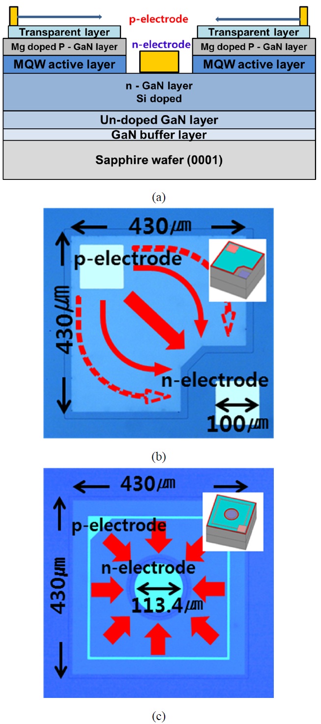
Figure 1(a) shows the schematic diagram of RT-LED for a GaN-based 460-nm blue LED. The epitaxial multi-layers were grown on the patterned sapphire substrate by using metal-organic chemical vapor deposition (MOCVD). It consists of a GaN buffer layer for the epitaxy process, un-doped GaN layer, Si-doped n-GaN layer, InGaN/GaN multiple quantum wells, and Mg-doped p-GaN layer. The thicknesses of n- and p-type GaN layers were 4 μm and 300 nm, respectively, and the doping concentrations were Si 3×1018 cm-3 and Mg 6×1017 cm-3. The exact atom fractions in InGaN in the quantum wells were 23% In and 77% Ga (In0.23 Ga0.77N). Each pair was composed of 3-nm In0.23Ga0.77N and 10-nm GaN, which made up a 65-nm quantum-well region by employing 5 pairs. As the transparent metallic layer for effective current spreading, a Ni (50 A)/Au (50 A) multi-layer was deposited on a p-GaN layer and then annealed by a rapid thermal process (RTP) at 500℃ in the N2/O2 ambient to form stable ohmic contacts [13-14]. A Ti (300 A)/Au (4000 A) multi-layer for electrode metal was deposited by an electron beam (e-beam) evaporator. The n-type electrode was formed on the mesa etched n-GaN layer at the center of the LED as show in Fig. 1(b) and a p-type electrode was formed on the p-GaN layer with rectangular ring type. The CV- and RT-LED devices were fabricated on the same chip and went through the same process conditions. Also, the areas of p-GaN layer (1.62×105 μm2), current spreading layer (1.39×105 μm2) and electrodes (104 μm2) of the RT-LED were designed to be the same as those of the CV-LED.
In designing an LED device, it is essential to extract the current spreading length from the material and process conditions and to utilize it as a design rule [15-16]. The distance between p- and n-electrodes of the RT-LED was also determined to be shorter than the current spreading length at the material conditions that we employed. The current spreading length is mathematically induced as follows [16]:
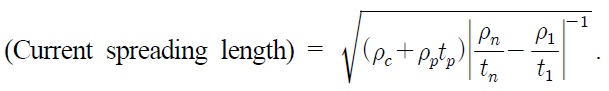
Here,
[18], and
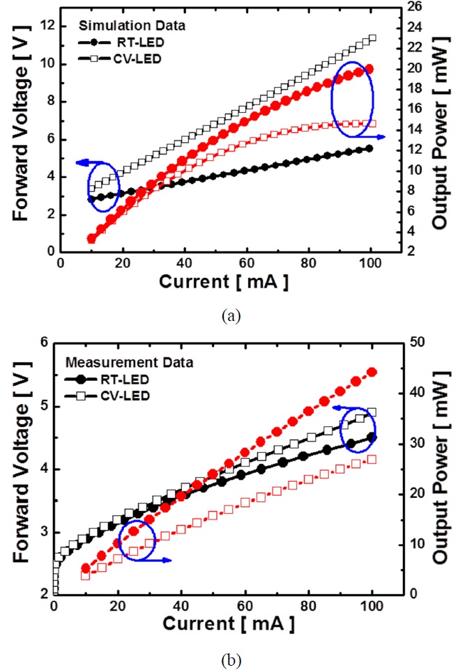
Prior to the LED fabrication, we investigated the performances of CV- and RT-LED by an optical simulation tool, SpeCLED [20]. Fig. 2(a) shows the simulated current -voltage (
the same, which, in consequence, reduced the actual area of p-electrode bonding pad (the left upper area where probing in the measurements is made). By this design approach, we could make the areas covered by the metals as well as the areas of active regions the same in both devices to make fair comparisons. Additional simulations revealed that local changing the p-pad area of RT-LED has little effect on current drivability. As shown in Fig. 2(a), the RT-LED shows higher optical power and necessitates lower forward operation voltage at all current levels than the CV-LED. Based on the simulation results, we investigated the performances of the fabricated RT-LED compared with those of the CV-LED. Fig. 2(b) shows the measured
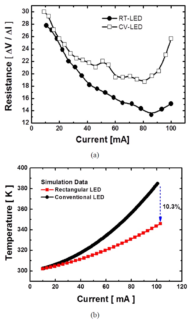
In order to confirm the directional uniformity of the injected currents, we observed the series resistance of fabricated LEDs. Fig. 3(a) shows the series resistance of CV- and RT-LEDs obtained by differentiations (
observed that that more current crowding in the CV-LED leads to higher series resistance due to interruption of current flow in the direction of the perimeter. The increase of series resistance due to non-uniform current also results in a rise in temperature of the LED [21-24]. As shown in the Fig. 3(b), the device temperature of the RT-LED predicted by simulation is about 343 K at 100 mA and it is 10.3% lower than 384 K of the CV-LED. Therefore, the RT-LED is operated with higher reliability in thermal perspective.
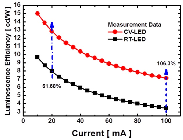
Figure 4 shows the luminescence efficiency of the RT-LED and the CV-LED. In this result, the RT-LED demonstrated improved luminescence efficiencies by 61.7% and 106.3% at two different current biases of 20 mA and 100 mA, respectively. The current flow in the RT-LED is distributed in every radial direction with the same distance between p- and n-electrodes, covering the whole device
surface and active region. Therefore, the electron-hole recombination extracting the light is drastically enhanced. Also, it is more probable that the light emission from the etched mesa sidewall is observed through both top and sidewall surfaces [3-4]. On the other hand, the local current -crowding in the small volume of region, for the case of the CV-LED, degrades the recombination rate.
In this work, we fabricated and demonstrated CV- and RT-LED devices. For more rigorous characterization of the designed RT-LED and its comparison with the CV-LED, the measurement analyses were accompanied by simulations. The electrode structures of the RT-LED led to uniform current spreading and reduced the series resistance. Through engineering the electrode geometry, RT-LED demonstrated higher electrical and optical performances. For wider commercialization of the RT-LED with centered island electrode, reliability issues such as short circuit-free wiring, degradation of external quantum efficiency, and failure by wire heating should be further studied.