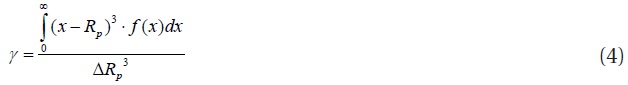
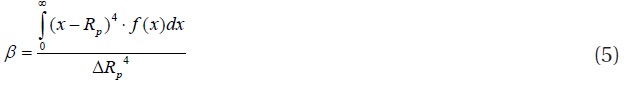
For the fabrication of CMOS devices, the retrograde wells of CMOS can be formed by using B, P and As ion implantations for p+ and n+ doping. For deep junctions, such impurities are implanted in silicon using an MeV implanter, and implanted wafers are annealed for electrical activation in N2 atmosphere. For the fabrication of power BICMOSFETs (bipolar complementary metal oxide semiconductor field effect transistors), accurate control of the depth profile is very important. Nowadays, SRIM (Stopping and Range of Ions in Matter) Monte Carlo simulations are widely used for the calculation of the implanted range in targets [1,2]. The physical effects of the slowing mechanism of implanted ions in silicon have also been examined extensively [1-10]. Experiments on implantations using MeV accelerators have been carried out for the fabrication of semiconductor devices, and the dynamics in implanted silicon have been analyzed using RBS (Rutherford Backscattering Spectrometry). The exact calculation of range in the MeV region is very important in semiconductor technology. However, some deviations in the ion range and defect formations between theoretical and experimental data have not yet been fully explained. TRIM (Transport of Ions in Matter) [1,2] was used as a Monte Carlo simulation tool for onedimensional profiles in various targets. Four moments were used for moment calculations in the one-dimensional (1D) vertical direction. The first moment Rp (projected average range) is the average range under normal implantation, the second moment ΔRp (standard deviation) represents the width of profile, the third moment γ (skewness) indicates the asymmetry of the profile, and the fourth moment β (kurtosis) represents the extent of the profile sharpness in the peak-concentration area. SRIM2013 output data was compared with measured SIMS data. [17]. For the moment calculations in the vertical direction, the following equations were used:

where Cdose is an implanted dose, C(x) is concentration as a function of the depth x, and

A Gaussian profile has only two parameters due to symmetry, and can be expressed as:
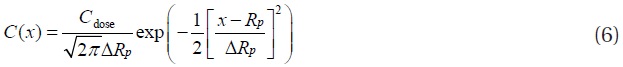
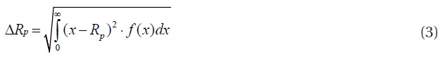
The projected average range (Rp) of a Gaussian profile is located near the peak concentration.
A Gaussian profile is generally not adequate to express asymmetry profiles for B-implanted, and P-implanted silicon. In the high energy region, the equations of electronic energy loss straggling and nuclear energy loss straggling can also be expressed as the equations below.
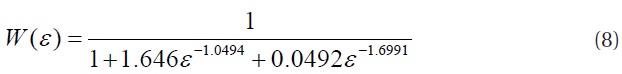
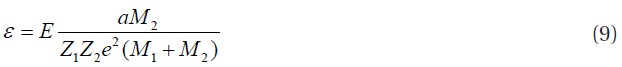
In the equation 8, ε is the reduced energy as described in equation 9.
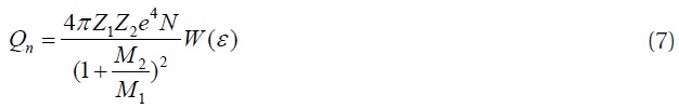
For low (L. E.) and high energy (H. E.) regions, Qe can be expressed as equation 10.
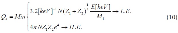
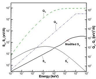
Where W(ε) is the analytical ZBL function, Z1, Z2, M1, M2, and E are the incident ion number, target atom number, incident ion mass, target atom mass, and incident ion energy, N is the target atomic density, e is the elemental charge, and a is the screen length, respectively. Qe is the electronic energy loss straggling. This straggling Qe is dominant, when a light element implanted silicon. In the experiments, only boron implant corresponded to the domination of Qe in silicon. Heavy elements in implanted
[Table 1.] Constants in the screening functions for various potentials
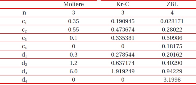
Constants in the screening functions for various potentials
silicon caused the ion distribution mainly through nuclear stopping power. The stopping power Se and Sn are defined as average energy. In an individual process, there is a statistically fluctuating energy loss in the ion implantation. In the high energy region, the equations of electronic energy loss straggling Qe and nuclear energy loss straggling Qn can also be expressed in equations 7 and 10, respectively.
The screen length can be expressed by equation 11.
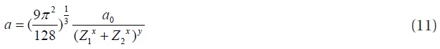
where α0 is Bohr’s radius.
In the high energy region of the TRIM program, the standard deviations in the projected direction can be expressed as:
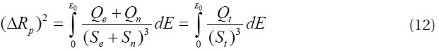
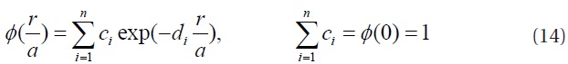
Three different models, the Firsov-, Lindhard et al.-, and ZBL (Ziegler, Biersack, Littmark) models [16,17], can be expressed as x=1/2, and y=2/3 for the Firsov-model, x=2/3, and y=1/2 for the Lindhard et al.-model, and x=0.23, and y=1.0 for the ZBL-model. The screened Coulomb’-potentials are expressed in equations 13, and 14, and in Table 1.
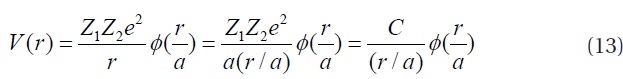
In MeV regions (r/a<1), the screening effects of various interatomic potentials are almost the same.
Therefore, the range parameters Rp and ΔRp are also almost the same value in the three potentials. Nevertheless, the range values after computer simulations were always shown with RZBL>RMoliere>RKr-C with very small differences in values. There were no differences in the range values between ZBL and Moliere potentials, but the range values of the Kr-C potential were somewhat smaller.
2. EXPERIMENTS OF B, P AND As IMPLANTATIONS
P-type silicon wafers-, doped with (100) boron and ρ values of 4-5 Ωcm-, were used. The concentration of the silicon substrate was about 3×1015 cm-3. For the p and n-type doping of retrograde well formations for CMOS fabrication, B, P and As ions were implanted in silicon wafers. Implantations into the silicon substrate
with different doses were carried out using a tandem ion implanter.
Before the implantation, the accelerated energies were calculated from the injection energy, charge state, and terminal voltage. The final implanted energy can be calculated using equation 15:

where Vinj, n, and VT are the pre-acceleration voltage (60 V), charge state of ions, and terminal voltage, respectively. A cesium (Cs+) ion sputtering source was used for the extraction of negative ions. The negative ions are attracted with the terminal voltage and the accelerated ions are collided with the N2-stripped gas in the middle zone. The negative ions can be changed into positive ions. After that, the positive ions are repelled again and focused through the electrical field lines with three quadrupoles.
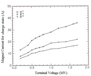
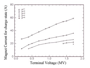
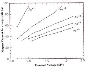
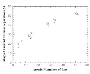
The vacuum inside the accelerator was 1×10⁻⁷ torr, and the space between the electrode and the tube was filled SF6 gas for electrical isolation. This accelerator has two magnets for the implantation and RBS. The first magnet was used for the mass separation in the injector parts and the second magnet was used for the separation of charge states in the front part of the end station.
The magnet current for the mass separation of various ions in the first magnet is shown in Fig. 1. The magnet currents for the charge separation of boron, phosphorus and arsenic ions in the second magnet are shown in Figs. 2,3 and 4, respectively.
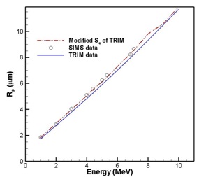
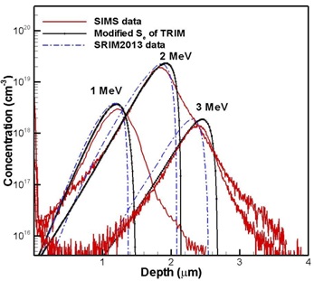
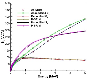
The modified electronic stopping powers of SRIM and SRIM2013 are shown in Fig. 5.
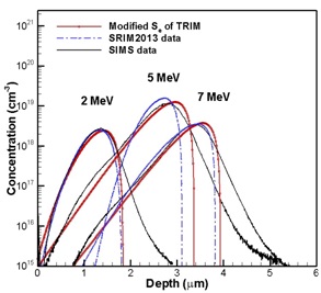
Boron, phosphorus, and arsenic ions implanted in silicon show somewhat shallower depth in the SIMS data. This means that the electronic stopping powers of SRIM are overestimated in implanted silicon. Based on this, the electronic stopping powers of SRIM are modified and optimized by comparing with measured SIMS data.
The fitted curves of boron-implanted silicon are obtained by the modification of the electronic stopping power of SRIM as follows;


where the energy E and electronic stopping power Se are in units of 1,000 keV and eV/Å, respectively.
The fitted equations could not be expressed as only one equation because of the broad energy regions from 1 to 10 MeV.
The fitted curves for phosphorus-implanted silicon are obtained by the modification of the electronic stopping power of SRIM in equations (19-21):


The fitted curves in arsenic-implanted silicon are obtained by the modification of the electronic stopping power of SRIM in equations (22-25):


where the energy E and electronic stopping power Se mean the unit of 1,000 keV and eV/Å, respectively.
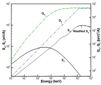
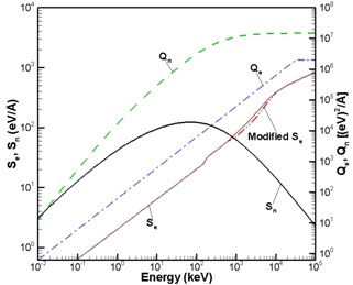
The electronic stopping power Se and nuclear stopping power Sn in B-implanted silicon are shown in Fig. 6.
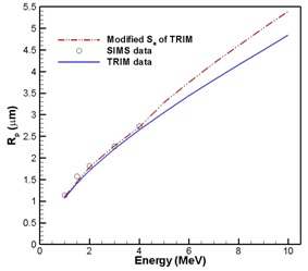
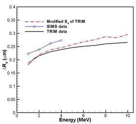
The value of Se was 87.62 eV/Å at 1 MeV, and 97.24 eV/Å at a peak point at 2.25 MeV. On the other side, Sn showed a very low value of 0.5814 eV/Å at 1 MeV, and continuously decreased gradually between 1 and 3 MeV. This means that Sn can actually be disregarded in MeV. The solid-dot-dot line in the figure shows a modified Se line, which has somewhat values than those obtained from TRIM data. The range data showed better results than the TRIM data using a modification of Se in B-implanted silicon. The TRIM data was obtained using SRIM 2013 [17]. For good fitting with SIMS data the somewhat lower values of Se than the Se of SRIM 2013 are corrected for the modifications of Se in B,
P, and As in implanted silicon. The measured SIMS data of B, P, and As in implanted silicon were slightly higher than the TRIM simulated data. The Sn and Se data can be used for the range calculation for implanted profiles. For this reason, the nuclear stopping power Sn of the ZBL model [17] was substituted with the Moliere and Kr-C models [16], and the simulated range data were very similar. The range data showed the best results using the ZBL model in comparison with the SIMS data. The Sn value of B in MeV implanted silicon could be disregarded due to very low values ranging from 0.5814 eV/Å at 1 MeV to 0.08734 eV/Å at 10 MeV in TRIM data. The electronic stopping power Se plays an important role in the MeV region, and can be modified from the original TRIM value. The changed curves are shown in Fig. 5 and 6.
The range data are also showed better results than TRIM data using a modification of Se in P-implanted silicon. The value of TRIM Se was 110 eV/Å at 1 MeV, and 294.5 eV/Å at 10 MeV, with a continuously increasing sloped line, as shown in Fig. 7. The peak Sn value of P implanted in silicon was 44.2 eV/Å at 15 keV. The value Sn of P was relatively low, ranging from 9.549 eV/Å at 1 MeV to 1.688 eV/Å at 10 MeV in TRIM data. The electronic stopping power Se can be modified from the original TRIM value. The changed curves in P-implanted silicon are shown in Figs. 5 and 7.
The electronic stopping power Se of TRIM is somewhat overestimated in the MeV region.
The range data showed better results than the TRIM data using a modification of Se in As-implanted silicon. The electronic stopping power Se can be modified from the original TRIM value.
The changed curves are represented as solid-dot-dot line for Asimplanted silicon in Figs. 5 and 8. The electronic stopping power Se is remarkably overestimated in the MeV region. The value of TRIM Se, which was 80.26 eV/Å at 1 MeV, and 383.3 eV/Å at 10 MeV, was a continuously increasing sloped line, as shown in Fig. 8. On the other hand, the Sn value of As showed relatively low values ranging from 62.49 eV/Å at 1 MeV to 14.36 eV/Å at 10 MeV in TRIM data.
The simulated results of range calculations were shown from Fig. 9 to Fig. 14.
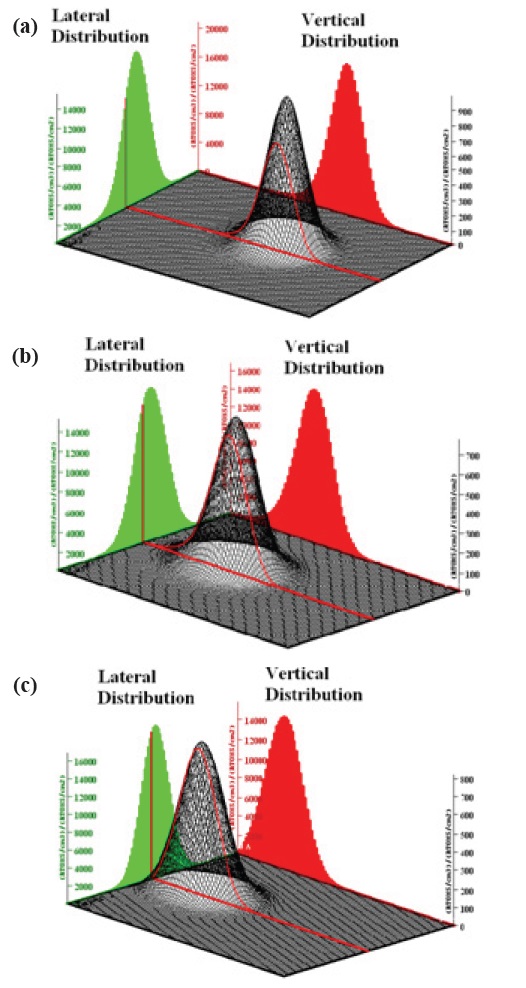
Three-dimensional B, P and As profiles of SRIM2013 are shown in Fig. 15. Every vertical length is 3 μm in all three profiles. The shapes of the three profiles differ in regard to the positions and distributions due to the different ion masses and scattering angles.
The three-dimensional profiles in B, P, and As implanted silicon are shown in Fig. 15.
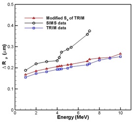
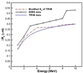
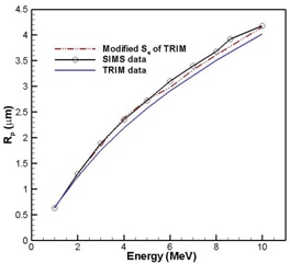
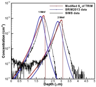
The positions of peak concentrations in the modified Se TRIM data are remakably improved in comparision with the SIMS and SRIM data in Figs. 16,17, and 18.
The percentage of the tolerance between the experimental and simulated data can be expressed by equation 26:
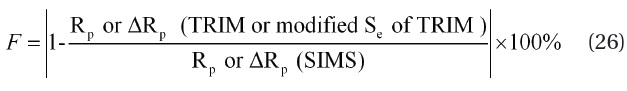
The calculated tolerances of Rp and ΔRp between TRIM and SIMS data in B-implanted silicon from 1 to 10 MeV were 5.53% and 20.5%, respectively. The calculated tolerances of Rp and ΔRp between the modified Se of TRIM and SIMS data were remarkably improved by 1.98% and 15.8%, respectively.
The calculated tolerances of Rp and ΔRp between TRIM and SIMS data in P-implanted silicon from 1 to 5 MeV were 3.77% and 16.8%, respectively. Those Rp and ΔRp between the modified Se of TRIM and SIMS data were remarkably improved by 1.44% and 13.8%, respectively.
The calculated tolerances of Rp and ΔRp between TRIM and SIMS data in As-implanted silicon from 1 to 10 MeV were 5.27% and 17.3%, respectively. The tolerances between the modified Se of TRIM and SIMS data were also remarkably improved by 2.64% and 15.3%, respectively.
The range parameters, Rp and ΔRp of B, P and As through the modifications of Se have been remarkably improved compared to results of SRIM2013, which has been continuously improved as a simulation tool since 1985. The range parameters of B, P and As obtained using ZBL potentials showed the best results among the various inter-atomic potentials (ZBL, Moliere, and Kr- C). In experiments, B, P and As ions were implanted into silicon. The MeV implanted data showed small discrepancies between SIMS and simulated data of SRIM 2013, the newest version of the simulation tool. The SRIM 2013 data provided values of the electronic stopping power Se of B, P and As ions in silicon that were somewhat overestimated. For this reason, the Se values of B, P, and As ions were modified to be slightly smaller, and the results of the calculation were optimized through modification of Se. In the MeV regions, the electronic stopping power plays a dominant role in comparison with nuclear stopping powers. The fitted Se equations could not be expressed as only one equation because of broad energy regions from 1 to 10 MeV in B, P, and As-implanted silicon. In the MeV, the electronic stopping power of B and P were proportional to E0.2 and E0.64 instead of E0.5, as expressed in the LSS stopping power model [11-15]. The electronic stopping powers of As were proportional to E0.5, as expected for the heavy ions. Through the modifications of Se in B, P and Asimplanted silicon, the range calculations were optimized and the range parameters showed better results than those of SRIM2013. The calculated tolerances of Rp and ΔRp between the modified Se of TRIM and SIMS data were also remarkably better than the tolerances between the TRIM and SIMS data.