Downscaled metal oxide semiconductor field-effect transistors (MOSFETs) have been in progress for several years and were displayed in the 2009 International Technology Roadmap for Semiconductors (ITRS) [1]. The scaled down MOSFET has many advantages, such as integration of chip density, low voltage operation, driving current enhancement, and so on [2]. However, the variations in the electrical characteristics of MOSFET are an inevitable phenomenon and it must be overcome. This paper focuses on the modeling and analysis of the electrical characteristics of the multi-finger MOSFET according to the drain voltage variation.
When the multi-finger MOSFET is operated by changing drain voltage, the electrical characteristics are affected. Due to scaling down and the driving voltage variation, the scaling variables and device parameters also became smaller. Thus, electrical characteristic variations will be primarily focused on drain voltage variation. In addition, the electrical properties are also analyzed by varying the gate width and length and the number of fingers. By observing these variations, the behavior of downscaled multifinger MOSFETs can be estimated via parameterization.
In this paper, the multi-finger MOSFETs are fabricated using a commercial 90 nm process to investigate the characteristic variations. To build the device model, a parasitic resistance extraction method is used. Here, the characteristic variations of threshold voltage (Vth), subthreshold swing (Ssub), drain induced barrier lowering (DIBL), transconductance (gm), and mobility (μFEmax) are analyzed where the drain voltage and the gate structures are varying at the same time.
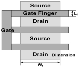
The multi-finger MOSFETs can be used in various applications since they have a large value of gm and it can control the current flow effectively. In addition, it can enhance the driving current because the multi-finger MOSFET has low gate resistance. Figure 1 is a basic schematic structure of a multi-finger MOSFET.
In Fig. 1, Lf is the length of gate, Wf is the width of gate, and Nf is the number of fingers. Thus, the total gate width of the tested
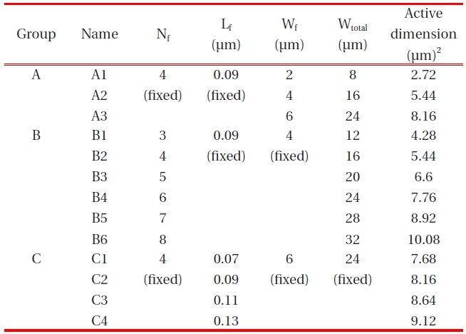
[Table 1.] Summary of the test structure information for each group.

Summary of the test structure information for each group.
MOSFET can be represented by the following equation:

In this paper, the test patterned multi-finger MOSFETs that change the gate structure are used to build a model and analyze the characteristics. Varying the gate width and length and the number of fingers was used to measure and investigate for variations.
The three groups of test structures are fabricated and used for analysis in this work. Here, group A consists of the test structures varying with the gate width, and group B consists of the structures varying with the number of gate fingers. It is noted that the total gate width of groups A and B are changed using different geometric factors. Finally, group C consists of the structures varying with the gate length. The group information can be summarized in Table 1.
The multi-finger MOSFETs used in this paper were manufactured in a common-source configuration. These test MOSFETs have a ground-signal-ground pad pattern that is designed with a pitch of 75 μm.
In order to measure the current-voltage characteristics, an HP 4145B semiconductor parameter analyzer was used. The measured data is stored with the aid of software and equipment. For the output characteristics (ID-VDS), the drain voltage is measured from 0 V to 0.9 V while the gate voltage is increased from 0.3 V to 1.2 V with a step of 0.3 V. In addition, the transfer characteristic (ID-VG) is derived by sweeping the gate voltage from 0.0 V to 1.2 V while the drain voltage is increased from 0.1 V to 0.7 V with a step of 0.2 V.
To extract the electrical characteristics of multi-finger MOSFETs, the parasitic resistance model is used in this paper [3]. In order to build the device model, a Berkeley short-channel insulated gate field effect transistor model 4 is based on the core
model. By connecting additional parasitic resistance for each terminal, it can complete the model. There are four different variables and they are optimized in the modeling process. The HSpice simulation program is used to extract the parasitic resistances via the ID-VDS output characteristic. The transfer characteristic is used to calculate Vth, DIBL, Ssub, gm, and μFEmax.
The sum of the optimized Rs and Rd is the total parasitic resistance that is calculated by using the extraction method. Rg is very small and it can be ignored because it is almost floating gate. Also, Rb can be ignored because the multi-finger MOSFET is fabricated in a common-source configuration.
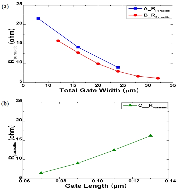
In Fig. 2, as the total gate width is increased, the parasitic resistance is reduced as the parasitic resistance is related to the operating current of the MOSFET. Here, equation of the parasitic resistance can be extracted, so it will be described as:
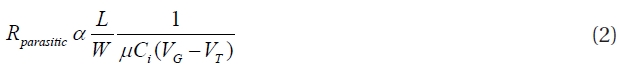
As a result of Eq. (2), the parasitic resistance is proportional to gate length, and is inversely proportional to gate width [4]. Both the gate width and the number of fingers change the total gate width, so it comes out with the same results.
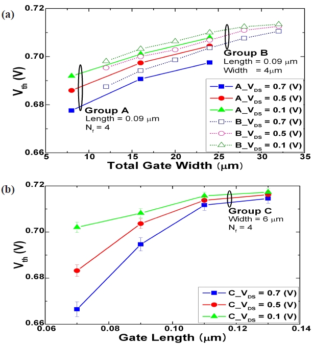
Threshold voltage is one of the most important characteristics of the MOSFETs. This paper extracted Vth from the transfer characteristic curve. The results of the extracted Vth are shown in Fig. 3.
From the results, the size of the MOSFET is reduced and the Vth decreases. In Fig. 3(a), both the number of fingers and gate width are reduced and Vth decreased gradually. It indicates that the variations of the gate width and the number of fingers have the same effects on Vth.
However, the variations in drain voltage affect Vth along with the change of the gate length. In Fig. 3(b), this reduction of Vth with a scaled down length is defined as the Vth roll-off since the
short channel effect occurs [5]. The fields of source and drain influence the channel, and as the dimension of the MOSFET decrease, the Vth roll-off phenomenon occurs on a large scale. Thus, it greatly affects the short channel on the potential profile [5]. In addition, the DIBL effect can also cause significant Vth roll-off.
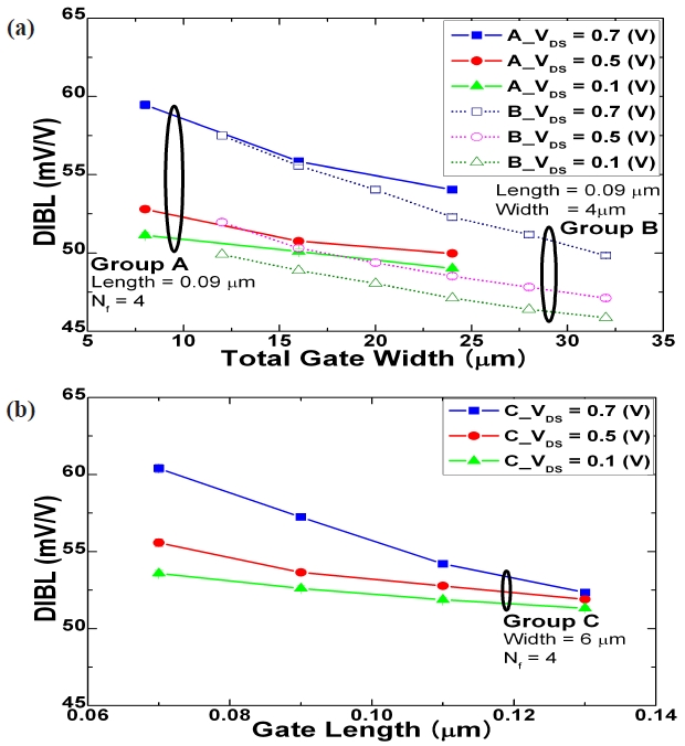
The results of the calculated DIBL of the multi-finger MOSFETs are presented in Fig. 4. In this paper, DIBL is calculated as ΔVG over ΔVD, where VD = 1.2 V and VG is ID = 0.1 μA/μm [6].
As mentioned, DIBL is one of the major reasons for Vth roll-off [5]. When a large drain voltage is applied, the DIBL is increased because the barrier is reduced between the drain and the source. DIBL can increase the drain current and it is proportional to the
applied drain voltage, thus DIBL is sensitive to drive voltage. As the size of the total gate width is increased, the dimensions of MOSFETs are increased and the DIBL is decreased in all three groups. The gap between the source and the drain is also increased. Thus, a large dimension prevents the drain field from penetrating the channel. It also prevents the potential barrier lowering [7]. The reduction of the DIBL in group B is much larger than group A because the dimension increment of group B is larger than that of group A. So, group B is less affected by short channel effects. In Fig. 4(a), the DIBL of group B also rapidly decreased compared with group A. Figure 4(b) shows that the dimension variation due to the change in length affects the DIBL. As a result, it has a high immunity about DIBL effect to use many fingers as the group B.
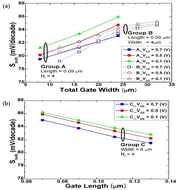
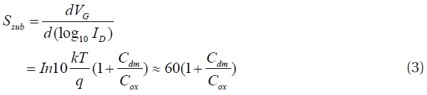
Ssub variation results are shown in Fig. 5. In general, Ssub is proportional to the total gate width and is inversely proportional to gate length. The following Eq. (3) expresses the Ssub:
In Fig. 5(a), the Ssub is gradually raised by increasing the total gate width. The depletion region and the value of the depletion capacitance (Cdm), which is a crucial factor for Ssub, are taken into account for analyzing the Ssub. From these results, if both the number of fingers and gate width are increased, the Cdm becomes large. As the depletion region is increased, the Cdm is also increased. However, Ssub of group B is larger than that of group A because the variation of Cdm through the change of the number of fingers is larger than that of change of the gate width.
In contrast, the Ssub decreases when increasing the gate length as shown in Fig. 5(b). Since the dimension of the MOSFET grows very large, the full depletion region is decreased, and the result is Cdm reduction [8].
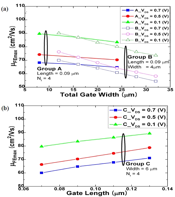
The gm is the ratio of the drain current changes to the gate voltage changes. In this paper, gm is defined as the maximum value
of the differential transfer curve. The μFEmax is proportional to gm, so μFEmax can be calculated from the following equation:

where Ci is gate capacitance per unit area. Figure 6 shows the calculated μFEmax of the multi-finger MOSFETs.
In general, if the total gate width is increased, the gm is increased. The gm is related to the flow drain current and the current is increased when the gate width is increased, which makes gm large.
However, in Fig. 6(a), the μFEmax is slightly decreased as the total gate width is decreased. The reason for this is that the size of the multi-finger MOSFETs has larger effects on the mobility than the transconductance. Also, the slopes of μFEmax of group B are larger than those of group A because the dimension variation of group B becomes larger than that of group A.
Conversely, for group C in Fig. 6(b), the three slopes of μFEmax are almost the same, which is a different trend than group A and B because the gate length variation of group C comes to change on a large scale, so it has dominant effects on the μFEmax.
The geometric variation effects depending on the drain voltage of the multi-finger MOSFETs were investigated in this paper. The electrical characteristics of multi-finger MOSFETs were extracted from the proposed model and used for variation analysis. The electrical properties, such as Vth, DIBL, Ssub, gm, and μFEmax, were analyzed depending on the drain voltage and gate structure variation. Thus, this modeling methodology allows us to provide the design guidelines for the gate geometric structure of the multi-finger MOSFET depending on the driving voltage for memory applications.