Several ferroelectric materials including Pb(ZrxTi1-x)O3 (PZT) and (Bi,La)4Ti3O12 (BLT) have been extensively studied to evaluate their feasibility as materials of ferroelectric capacitors to be applied in ferroelectric random access memory (FeRAM) [1-4]. The BLT material has many advantages over the PZT material [4-6], such as being fatigue-free on platinum electrodes and having long term reliabilities such as imprint [3,7-9]. In addition,the BLT material having a Bi-layered perovskite structure has strong anisotropy of polarization values [8,10-12]. Therefore, crystallographic orientations in BLT films must be controlled to maximize the polarization value. Uniform grain size must also be obtained to improve the cell-to-cell uniformity of the polarization value. Recently, we reported that the orientation of the BLT film coated with a metal-organic decomposition (MOD) solution can be controlled by optimization of process conditions [8,13,14]. Extremely narrow window of process conditions gave random-oriented small BLT grains [13,14], which were suitable for high density FeRAM devices. This critical issue of the abnormal grain growth to c-axis was the reason for the evaluation of the physical vapor deposition (PVD) method of the BLT film. In this study, both the microstructure and ferroelectric properties of PVD-BLT films were evaluated in a FeRAM cell structure.
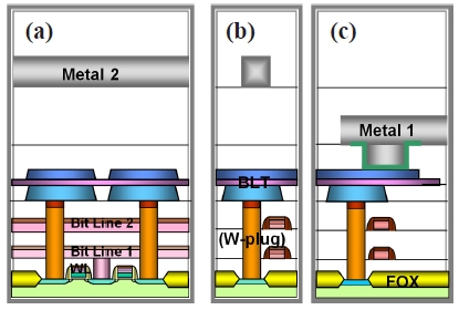
Figure 1 shows the cell structure for a high density FeRAM device [14,15]. The main feature of the novel cell structure, which is called as merged top and plate line (MTP) cell scheme, is that the top-electrode also serves as plate-line and extends in the word-line direction. The key processes of cell structure integration are briefly described in Table 1. A bottom electrode stack of Pt/IrOx/Ir (100 nm/10 nm/150 nm) was deposited by the sputtering

Integration process features of the ferroelectric random access memory device with the novel cell structure of a merged top and plate line.
method on a buried TiN barrier. The stack was isolated by using a conventional etching process. And then, the patterned bottom electrode was buried in the inter-layer dielectric film by an oxide chemical mechanical polishing process. A 100-nm-thick BLT thin film was deposited on the buried bottom electrode stack by the pulsed-DC sputtering method (PVD-BLT). The starting composition of the sintered BLT sputtering target was Bi4.8La1.0Ti3.0O12. The target composition was predicted with the results from a previous experiment on the MOD-BLT solution because no data based on the pulsed-DC sputtering deposition method were available for the BLT thin film. The Bi and La content in the PVD-BLT target were excessed to obtain the BLT film composition of Bi3.25La0.75Ti3.0O12, which was the optimized composition with the MOD-BLT solutions [9,11]. The process conditions for PVD-BLT layer deposition were as follows: deposition temperature of 250℃, deposition power of 400 W, working pressure of 1.8 mTorr, and Ar/O2 gas flow rates of 35 sccm/4 sccm. The as-deposited PVD-BLT thin film was annealed at 560℃/O2/6 min with rapid thermal process (RTP) to densify it. Then, the film was fully crystallized at 700℃/O2/30 sec with the same RTP equipment.
The crystalline orientation of the BLT film was examined by using X-ray diffraction (XRD) with a Cu-Kα radiation source. And the microstructure of the BLT films was inspected by both a scanning electron microscope (SEM) and a transmission electron microscope (TEM). Electrical properties such as contact resistance
and ferroelectric properties of the BLT capacitors were evaluated after integration up to the metal-2 layer in accordance with the conventional process flow of a FeRAM device as described in Table 1.The ferroelectric properties such as polarization and fatigue loss were measured by using the RT6000SI ferroelectric tester (Radiant Technologies, USA).
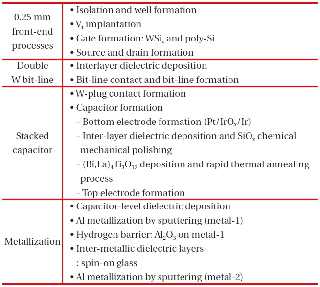
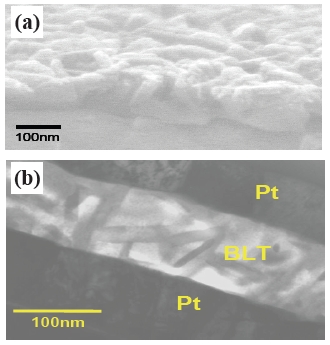
Thermal stability issues such as sidewall oxidation have been common in a conventional TiN barrier interposed at the interface between the oxygen barrier (Ir) and the W-plug [15]. Therefore,to obtain a robust plug structure, the buried TiN barrier was fabricated on the recessed W-plug [9]. The buried TiN barrier structure under the stacked Pt/BLT/Pt/IrOx/Ir capacitor is shown in Fig. 2 . Figure 2(a) is the cross-sectional SEM image and Fig. 2(b) is the TEM image of a novel cell structure. Sidewall oxidation was not observed even after full integration up to metallization [15].
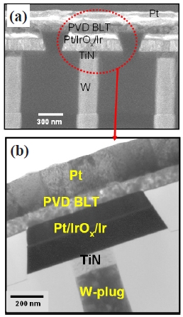
Figure 3 shows the resistance properties of the storage node contact. Figure 3(a) is the current-voltage curve measured at one W-plug test pattern and Fig. 3(b) is the distribution of the contact resistance measured at the 1,024-contact chain pattern. The linear current-voltage relation shown in Fig. 3(a) proves the ohmic contact from the bottom electrode to the source region of the transistor. And the contact resistance values have very narrow distribution as shown in Fig. 3(b). In other words, the W-plug showed the low contact resistance of ~400 Ω/plug at Φ0.25 μm contact size.
The BLT films were deposited by the sputtering method on a buried bottom electrode stack of Pt/IrOx/Ir. The major issue in the deposition of the BLT films to realize high polarization was the orientation control of each grain because of the strong anisotropy in electrical polarization [7,8,12]. The saturation polarization value (Ps) is small (~4 μC/cm2) along c-axis, but large(~50 μC/cm2) along a-axis or b-axis [10,12]. That is, the grain orientation in the BLT film must be aligned to the a-axis or baxis to maximize the polarization value. However, the MOD-BLT films showed a strongly c-axis orientation, which resulted in the lowest polarization value. The c-axis orientation of the MOD-BLT films is affected by the orientation of the Pt electrode surface. And the electrode effects on the MOD-BLT films may be strongly related with the nucleation stage of the BLT grains during the
post-annealing process performed after the spin-on coating of the MOD-BLT solution. The MOD route may follow these steps: (1) spin-on coating, (2) decomposition of the MOD solution (the Bi, La, Ti may exist as separate atoms without chemical bonding), (3) nucleation for the BLT grain, and (4) grain growth at the nuclei.
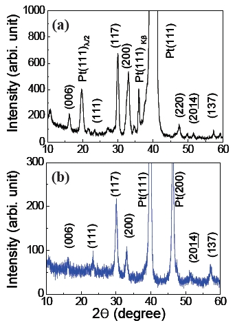
These critical orientation and grain size issues in the MODBLT films were the main reason for evaluating the PVD method for BLT film deposition. The crystallographic orientation of the PVD-BLT film analyzed by XRD method is shown in Fig. 4(a). As the reference in the analysis of the BLT film orientation, a specially fabricated BLT powder was also analyzed and its data is shown in Fig. 4(b). The BLT powder used as reference was fabricated as follows: (1) the BLT layer was coated on the Pt bottom electrode, (2) crystallization annealing was carried out at 700℃/O2/30 sec, and (3) the BLT thin film was stripped off by scratching with a knife. Finally, the BLT powders containing some Pt powders were made by the soft grinding method of the stripped PVD-BLT thin film. The major diffraction peak of the PVD-BLT film was the direction of (117), which was similar to that of the reference BLT powder shown in Fig. 4(b). This similarity implies that the grains in the PVD-BLT film have a crystallographic ran-
dom orientation. The random orientation in the PVD-BLT thin film may be related with the nuclei generated during the deposition process. That is, the PVD-BLT films may be deposited as nano-particles, not as separated ions or atoms. Nano-particles would show random orientation regardless of the orientation on a Pt electrode surface. And they would act as nuclei of the BLT grains during the post-annealing process. That is, the PVD-BLT grains can increase in size without the nucleation step. These behaviors may be the reasons why the PVD-BLT film showed random orientation.
Recently, we reported that the orientation of the MOD-BLT film can be controlled by optimizing the post-annealing process conditions [13,14]. But, the window of the process conditions was too narrow for obtaining randomly oriented small BLT grains [13,14], which are needed for high density FeRAM devices. However, we could easily deposit PVD-BLT films having grains of random orientation, as shown in Fig. 4.
Figure 5(a) is the SEM image of the PVD-BLT surface observed after crystallization annealing at 700℃/O2/30sec, and Fig. 5(b) is the cross-sectional TEM image of the PVD-BLT capacitor inspected after deposition on the top Pt electrode. The BLT layer has uniform, small, and ellipsoidal-shaped grains (long direction:~100 nm, short direction: ~20 nm). The c-axis oriented large grains, which caused the failure of the cells in the real FeRAM devices fabricated with spin-coated MOD-BLT thin films [13,14], were not observed in the PVD-BLT films.
The electrical properties were measured via W-plug after integration up to metallization with aluminum. The ferroelectric hysteresis loop was obtained from 32 k-array capacitors (the number of capacitor: 32 × 1,024 each, unit capacitor size: 0.7μm2). The remnant polarization (2Pr) value was about 21 μC/cm2, which was high enough for FeRAM devices. The leakage current density of the PVD-BLT capacitor was about 3 × 10⁻⁵ A/cm2 at the applied voltage of 3 V. It was higher than that of the optimized MOD-BLT films [7,8]. Therefore, we analyzed the composition of the PVD-BLT layer by using the inductively coupled plasma method. The composition in the deposited PVD-BLT film was Bi4.0La1.0Ti3.0O12 after heat treatment. Both Bi and La contents were higher than those of the optimized MOD-BLT film, whose composition was Bi3.25La0.75Ti3.0O12. The excess Bi and La contents in the deposited PVD-BLT film may be the primary reason for the higher leakage current density. So, in future studies, the composition for the PVD-BLT film should be optimized by lowering the Bi and La contents in the composition of the BLT sputtering targets.
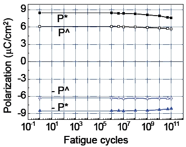
Figure 6 shows the fatigue loss of the deposited PVD-BLT film. The applied signal was 1 MHz bipolar pulse with 3V maximum voltage. The PVD-BLT film showed similar fatigue loss of about 10% after 1 × 10¹¹ cycles as the optimized MOD-BLT film.
A stacked BLT capacitor with the novel MTP cell structure was successfully developed with the PVD-BLT thin film for a high density FeRAM device. The W-plug showed uniform low contact resistance of about 400 Ω/plug at Φ0.25 μm contact size. Both microstructure and ferroelectric properties of the PVD-BLT films were also evaluated in the newly developed MTP cell structure. The PVD-BLT layer showed the random orientation in crystallographic direction and had small and ellipsoidal- shaped grains. The remnant polarization (2Pr) and the leakage current density were about 21 μC/cm2 and 3 × 10⁻⁵ A/cm2 at 3 V, respectively. The fatigue loss was about 10% of the initial polarization value after 1 × 10¹¹ fatigue cycles. In conclusion, the PVD-BLT film is a very promising candidate as a ferroelectric layer for high density Fe-RAM devices because its small grains in random orientation can be easily deposited by the pulsed-DC sputtering method.