Copper (
The
Moore’s law by stacking chips vertically. Thus, copper interconnection has already assumed an important role in semiconductor device and packaging manufacturing.
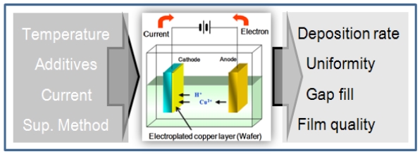
A number of variables must be considered in the electrochemical deposition of copper, such as seed layer coverage, base and additive chemistries, electrical power supply waveforms,temperature, humidity, and others. In the early stages of process development, PCB-based process chemistry was expanded to optimize the electrochemical deposition process for applying dual-damascene interconnection technology to advanced semiconductor fabrication [3]. During this time, a group of researchers at Stanford reported several findings: 1) electromigration lifetime of (111) CVD
In electrochemical deposition processes, the type and flow of the current source are known to be important factors for achieving desired film quality. However, bath chemistry including additives and impurities adds complexity to wet deposition process control. The simplified process inputs and responses of interest are illustrated in Fig. 1. To achieve successful
The objective of this paper is to facilitate the VM-APC by investigating optical transmittance spectroscopy (OTS) data from wet plating baths for the feasibility of real-time in-situ optical monitoring in the electrochemical copper deposition process. In this research, we practiced an optical non-invasive monitoring technique using three types of optical monitoring tools: chromatic sensors, UV/VIS spectroscopy, and near infra-red (NIR) spectroscopy. The motivation for the suggested optical monitoring technique originated from well-established in-situ plasma process monitoring methods. A chromatic monitoring sensor was used for real-time monitoring of the chamber arcing in the plasma etch process; UV/VIS spectroscopy, known as optical emission spectroscopy, has been used for real-time monitoring for malfunction diagnosis in plasma etch equipment [10]; and NIR spectroscopy measurement was used for real-time monitoring of the etching solutions [11]. The capability of chromatic monitoring of electrochemical copper deposition processes in advanced semiconductor manufacturing has been successfully demonstrated.
Section II illustrates the experimental apparatus and process mechanism, and Section III presents the in-situ real-time monitoring technique with the acquired data analysis. A correlation study with surface analysis results for the in-situ data is provided in Section IV, followed by the conclusion.
2.1 Electrochemical deposition process
Electrochemical deposition, also known as electroplating, is the deposition of a metal film onto an object by applying a negative charge to the object and immersing it into a solution that contains a metal salt. The metal salt contains positively charged metal ions which are attracted to the negatively charged object. Simple electroplating is a common school project that involves plating a copper coin with either copper or nickel. Positively charged polyatomic ions (cations) move to the cathode while negatively charged polyatomic ions (anions) move to the anode as a result of the conversion between electrical and chemical energy. When external electrical energy is provided, the metal at the anode is oxidized from the zero-valence state into cations and dissolves into the electrolyte. The cations are reduced at the cathode by depositing and settling to a metallic, zero-valence state.
In electrochemical copper deposition, copper is oxidized at the anode into
The electrolyte is a copper sulfate solution;
At the cathode (wafer), either
The final REDOX reactions are
2.2 Experimental setup and in-situ process monitoring sensors design of experiment
Dehydrated copper sulfate (
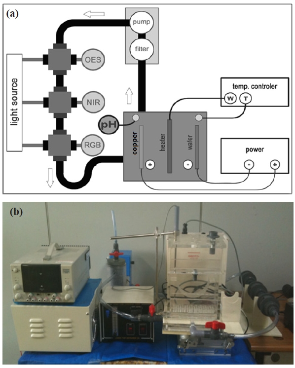
A custom-built electrochemical copper deposition system is used for this experiment. The bath can hold up to 6 inches of copper source and 4 inches of wafer. No wafer rotation was performed in this experiment, but the wafer holder can be rotated with the addition of a rotating unit for improved film uniformity. Bath temperature is controlled by a tungsten heater located at the bottom of the bath housing, and an industrial pH meter is also installed for the purpose of conventional chemical monitoring. The speed of solution circulation is controlled by an externally located circulation pump with a filter unit for sludge filtering, and an air bubble supply is also provided at the bottom of bath to minimize the effect of localized vortices in the solution. An illustration of the experimental apparatus is presented in Fig. 2.
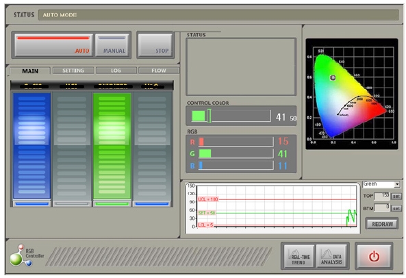
Three types of optical monitoring sensors are installed between the pump-out and bath-supply for optical transmittance spectroscopy (OTS). Each sensor unit is specially designed for its optical transmittance measurement with a glass cylinder type waveguide. Carefully designed optical waveguides immersed in the solution provide stable and reliable optical transmittance characteristics for in-situ chemical monitoring. The chromatic monitoring system consists of a sensor module with optical broadband detectors, a data acquisition hardware module with 1Hz sampling rate, and a computer monitoring system with integrated graphic user interface (GUI) as shown in Fig. 3. Chromatic
measurement provides not only color information in red, green, and blue levels, but also hue, saturation, and value information. Although chromatic data may not present scientific analytical
information on the object being monitored directly, it is sensitive to the change of color in the chemical solution during a continuous electrochemical copper deposition process. Detecting shift or drift and variation in the chromatic information also supports the potential of the system as an in-situ chemical monitoring technique.
Other sensors installed are UV/VIS and NIR spectroscopy devices.UV/VIS/NIR optical absorption, transmission, and reflectance (ATR) spectroscopy are useful methods for chemical analysis of molecular aggregation, orientation, and structure [12,13]. Optical emission spectroscopy (OES) has been actively employed as an in-situ monitoring tool for plasma diagnostics and process monitoring for more than a decade [14,15]. Spectroscopic monitoring sensors may provide more detailed information on the object being monitored by correlating specific peaks with atomic and molecular characteristics; however, in contrast with plasma processes, chemical solutions do not emit light, thus we have included-connected high-power tungsten-halogen light sources to employ OTS. Individual sensor units are optically isolated to prevent any optical interference by waveguide effects. In addition to optical monitoring sensors, conventional pH measurement was also set up to record the pH value of the hydrated sulfate solution.
After filling the bath with 4.5 L of
3. IN-SITU COLOR MONITORING OF PLATING BATH
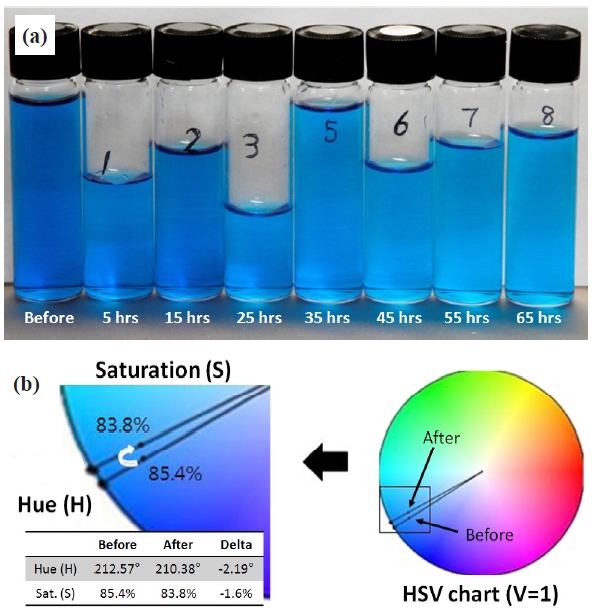
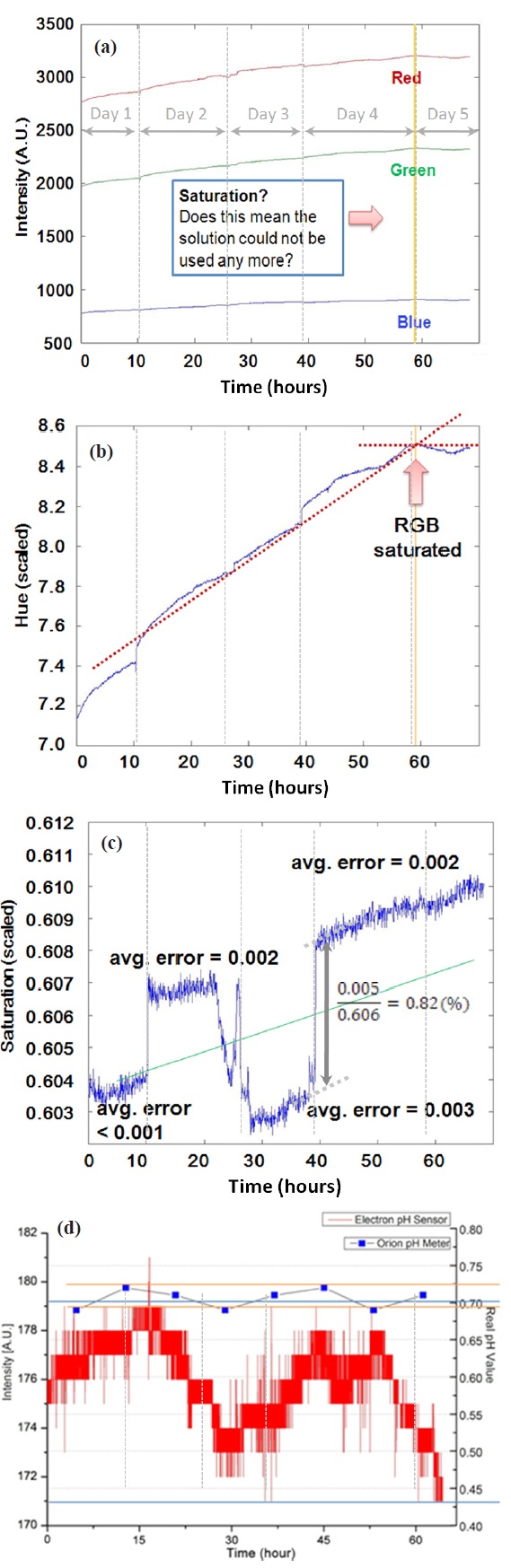
Sulfate solution was sampled every 10 hours to visually confirm our postulation of chromatic information changes in the redox process, and the collected samples are presented in Fig. 5(a). It is difficult to tell the difference between adjacent samples within 10 hours, but differences between the 3-4 samples are apparent in the figure. Converting RGB data to Hue-Saturation-Value (HSV), we have observed a decrease in hue by 2.19 degrees and saturation by 1.6% as shown in Fig. 5(b). The result proves what we have visually observed from the sulfate samples. We further investigated in-situ chromatic data with regard to whether the material’s optical properties were shifted or drifted over 70 hours of processing. As shown in Fig. 6(a), RGB representation shows a gradual increase in intensity of the three chromatic components, which were saturated around 58 hours. Scaled absolute values of hue and saturation are also presented in Figs. 6(b) and (c). We had the same observation as shown in RGB, and more clear saturation was observed in Hue. Figure 6(c) is shown to have a large amount of fluctuation in saturation; however, the largest fluctuation that occurred only contributes approximately 0.82% variation with respect to the baseline, and good agreement
was observed over course of the experiment. It is surprising that the chromatic intensity accurately detected every intermission of less than a half day, and it shows how chromatic monitoring can be sufficiently sensitive to the process variation. When comparing with real-time in-situ pH measurements and eight instances of augmented off-line pH measurements with Orion’s bench-top pH meter, no significant anomaly in the process was observed as shown in Fig. 6(d). Further explanation of the drifted optical monitoring data with wafer metrology will be provided in the next section.
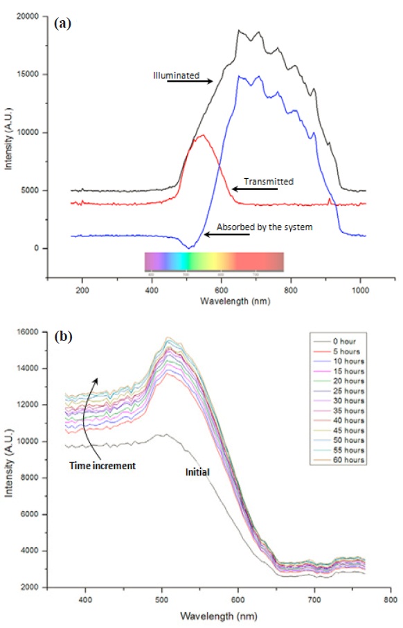
We recorded the optical transmittance spectroscopy (OTS) data from the empty system as a dark signal, and the absorbed signal was found by subtracting the acquired signal from the illuminated as shown in Fig. 7(a). UV/VIS spectroscopy data in the 350-550 nm wavelength range showed gradual increase along with increases in the process time, which is presented in Fig. 7(b). This is the same observation as in the previous chromatic result.In our postulation, we expected some noticeable peaks that would correspond to the chemistry as in plasma process monitoring; unfortunately no further detailed information was found in the acquired spectroscopy data from this experiment.
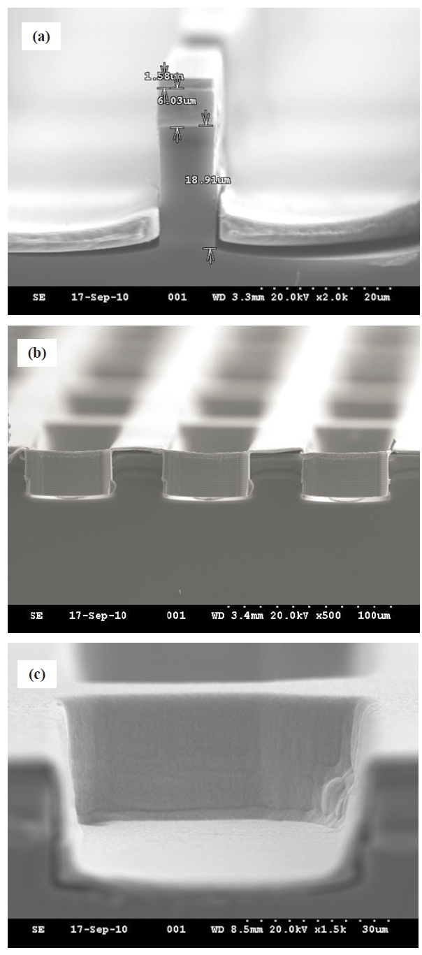
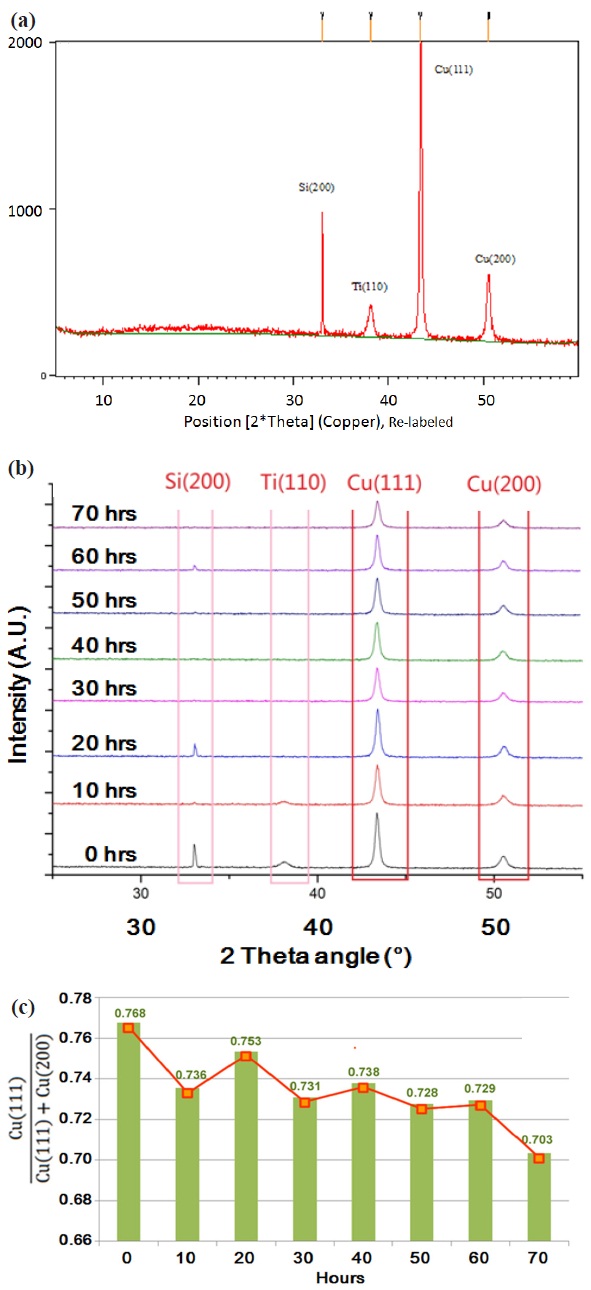
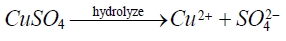
Although in-situ real-time optical monitoring revealed and identified color changes in the hydrate sulfate during the copper deposition, a direct relationship between the color change and film quality on the wafer is still in question. To alleviate this concern,sample wafers at every 10 hours of deposition processing were analyzed by scanning electron microscopy (SEM) and X-ray
diffraction (XRD) to characterize the surface and microstructure of the film. Fig. 8(a) shows the deposited wafer sample at 30 hours with AZ 5214 photoresist mask. We can clearly see that electrochemical copper deposition was successfully performed with a thickness of 1.58 ㎛. The wafer samples employed in this experiment were continuously recycled after stripping the electroplated copper layer off due to the limited resources of a university research environment. The repeated copper stripping caused PR erosion after the third day of the experiment, but consistent electrochemical deposition was performed for real-time monitoring without a PR layer. Figures 8(b) and (c) are crosssectional SEM images of the partially filled square vias acquired at 60 hours without a PR mask layer. The cut edge in the image presents scallop patterns from the Bosch trench process, and the deposited copper is comparatively uniform. The electrochemi-
cally deposited copper layer in Fig. 8(c) may show some amount of delamination because no adhesion layer was used for the silicon-copper interface. Otherwise, our CED process was generally successful. We also measured the thickness of the deposited copper at 10 and 20 hours, and the measured thicknesses were gradually decreased to 1.78 and 1.68 ㎛. The decrease in deposited thickness agrees with the degradation of the bath in the redox process, which is represented in color change of the hydrate sulfate solution.
Metal grain structure is also a critical factor for copper as a semiconductor interconnection material. (111)
It is desired to analyze the preferred orientation of the deposited metal thin layer in the same thickness because of the grain growth mechanism. Random nucleation allows a variety of growth orientations in the beginning of deposition process, and the grains with lower surface energy or higher growth rate (which is (111) in
Optical monitoring methods including chromatic monitoring and optical transmittance spectroscopy were demonstrated used for in-situ real-time monitoring of the electrochemical copper deposition process. Process variables to be controlled in the process are numerous, and the condition of the chemical solution in a plating bath is one of them. Conventional monitoring of chemical solution relies on the pH value of the solution, electrical voltage level by oxidation-reduction, and gravity measurement by immersing sensors into a plating bath. However, we employed an optical non-intrusive monitoring technique using three types of optical process monitoring tools, such as chromatic sensors and UV/VIS/NIR spectroscopy to develop a technically feasible optical monitoring method. This research is motivated by the fact that as the concentration of the copper cations (