Transparent conductive oxide (TCO) thin films, exhibiting both high electrical conductivity and optical transparency in the UV-visible region, have been studied for various transparent electronics applications, such as solar cells, liquid crystal displays (LCD), organic light emitting diodes (OLED), and touch display panels [1-3]. Among TCO thin films, tin oxide (SnO2) -based thin films have drawn significant attention, due to their low electrical resistance, associated with high optical transparency in the visible region, and high stability in mechanical and chemical resistance [4,5].
The most widely used materials system of TCO thin films for current transparent electronics is indium tin oxide (ITO) thin film, which has good electrical conductivity (~10-4 Ω·cm), and optical transparency (~90% in the visible range) [6,7]. However, the major component, indium, is one of the expensive rare earth materials components, and will face shortages of natural resources. In order to resolve this drawback in ITO transparent conductors, various materials systems are introduced as a TCO for the replacement of ITO [8-13]. Recently, it is reported that electrical conductivity is significantly increased for doped SnO2, as well as charge carrier concentration [14,15]. In particular, the donor elements in SnO2 (which have higher ionic valence than Sn (ionic valence +4)), are most commonly used to obtain high n-type conductivity, as well as high optical transparency. In this regard, the group V elements (ionic valence +5) doped SnO2 thin films have been explored for the replacement for ITO [16,17]. Moreover, it was reported that both film qualities and electrical properties are significant, depending on the deposition methods, such as chemical solution deposition, spray deposition, chemical vapor deposition (CVD) and sputtering, and so on. But for mass-producible and cost-effective manufacturing, TCO thin films need to be processed by the low-cost and large area massproducible solution-based deposition method, even though they have slightly lower electrical and optical properties, because film qualities can be enhanced, by controlling the process conditions and appropriate dopant selection [18-20].
In this paper, we have introduced antimony (Sb) as a donor element into the SnO2 matrix system, and investigated both the electrical and optical properties as a function of the Sb doping concentration and process conditions (annealing temperatures and environments). Our Sb-doped tin oxide (ATO) thin films have been prepared by using spin coating, with a non-alkoxide sol-gel derived stock solution. A non-alkoxide precursors incorporated stock solution is comparatively cheap and convenient in handling and usage during the sol-gel processing and film deposition, due to the environmental insensitivity of non-alkoxide precursors [21]. Finally, we investigate the crystallinity, microstructure, electrical properties and optical properties of ATO thin films in detail.
The precursor solution was prepared using SnCl2·2H2O (98%, Aldrich Chemical Co. Inc.) and SbCl3 (99%, Aldrich Chemical Co. Inc.) as starting materials, and 2-methoxyethanol (99%, Aldrich Chemical Co. Inc.) was used as a solvent. The mixture was stirred for 3 hours at room temperature (RT), to obtain a homogeneous stock solution with 1.0 M sol concentration. ATO thin films were deposited on a glass substrate (1737 non-alkali), using a spin coating method with a rotation speed of 4,000 rpm for 30 seconds. The as-deposited films were baked at 150℃ for 5 min on a hot-plate in an atmospheric environment. These coating and baking processes were repeated 3 times, to obtain the final film thickness of 200 nm. Then, the amorphous films were annealed at 350~650℃ for 30 min in a tube furnace. The annealing atmospheres were varied, as O2 (strongly oxidized), low vacuum (weak oxidized), high vacuum (weak reduction) and 10%H2-90%Ar (strong reduction) atmosphere. The film crystallinities were observed by using X-ray diffraction (XRD, D/MaX-2500, Rigaku), with Cu Kα radiation. Surface morphologies and thickness of films were examined by using a scanning electron microscope (SEM, S-4100, Hitachi Ltd.). The electrical property was measured by using a 4-point probe and Hall measurement (HL 5500 Hall system, BIO-RAD). The optical property was measured by using a UV-visible spectrophotometer (UV-160A, Simadzu), and UV-visible-NIR spectrophotometer (Cary500, Varian).
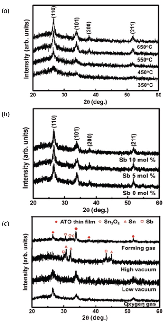
Before Sb doping, to obtain the appropriate processing temperature for well crystallized SnO2 thin films, we investigated the crystallization behavior of pure SnO2 thin films, as a function of annealing temperature. The XRD patterns of undoped SnO2 thin films on glass substrate are shown in Fig. 1(a). XRD patterns indicated that the thin film for an annealing temperature of 350℃ was an amorphous phase, and the crystallization of the film started at 450℃. The peak intensity was not clearly changed under 450℃, but (110), (101) and additional (200) and (211) peaks in the diffraction pattern were observed, with increasing annealing temperature over 550℃. No significant change occurred in intensity and orientation at a temperature above 550℃. From this result, the anneal temperature of ATO thin films was fixed at 550℃, in the investigation of Sb doping and the an-
nealing environment effect. Figure 1(b) shows XRD patterns of ATO thin films as a function of Sb-concentration at an annealing temperature of 550℃. XRD patterns of ATO thin films show a single phase, without secondary phases and random orientation (JCPDS reference card #41-1445). Moreover, no change and shift was observed in diffraction patterns by a doping effect of up to 10 mol%, similar to other reports [22,23]. However, the crystallinity of ATO thin films were considerably affected by the annealing atmosphere (especially in a reduction atmosphere), as shown in Fig. 1(c). XRD patterns of ATO thin films prepared under an oxygen atmosphere and low vacuum obtained a single phase without secondary phases, although those of ATO thin films prepared under high vacuum and 10% H2-90% Ar forming gas show a weak crystallization, and secondary phases, such as Sn, Sb, and Sn3O4. From this result, we suggest that insufficient oxidation of ATO thin film can be caused by an oxygen deficient atmosphere during annealing under high vacuum and forming gas, and as a result, a weak crystallization and secondary phases in ATO thin films might be caused.
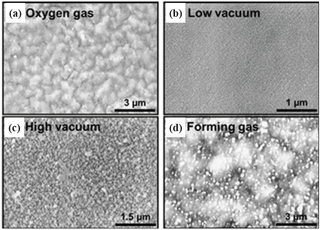
Surface morphologies of ATO thin films were monitored by scanning electron microscopy (SEM). Although the surface morphology as a function of Sb-concentration was not apparent, it was considerably affected by the annealing condition. Surface
morphologies of 5 mol% Sb doped SnO2 thin films, as a function of annealing condition, are shown in Fig. 2. Those of ATO thin films prepared under an oxygen atmosphere and low vacuum pressure show smooth and dense surface morphology, as shown in Figs. 2(a) and (b). However, ATO thin films prepared under high vacuum pressure and forming gas show a distinct surface morphology, and excessive number of particulate defects with hazed thin films, as shown in Figs. 2(c) and (d). It was considered that this result of hazed colored surface morphologies by annealing condition might be caused by a weak crystallization, with secondary phases in the ATO thin films prepared under low vacuum and forming gas, as mentioned above. It is expected that modification of the surface morphology of ATO thin films might affect the optical properties.
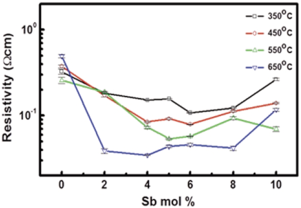
Figure 3 shows the characteristic of electrical resistivity in ATO thin films as functions of annealing temperature and Sb-concentration. Electrical resistivity is decreased with increase of Sb concentration and annealing temperature. In improved electrical resistivity, these might offer some possibilities, such as doping effect, crystallization quality and grain boundary, compared to that of pure SnO2 film. We suggest that for ATO thin films, carrier concentration might be increased by increasing Sb-concentration, and decrease of resistivity might be due to crystallization
quality, and decrease of grain boundary density by increasing annealing temperature.
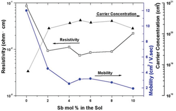
Figure 4 shows the results of Hall measurement as a function of Sb-concentration in ATO thin films. By increasing Sbconcentration up to 8 mol%, resistivity and mobility gradually decreased, while carrier concentration increased. This indicated that the conductivity of thin films was enhanced by the doping effect of Sb in SnO2 films. For TCO thin films, it has been reported that doping of donor elements and annealing under forming gas are required to enhance carrier concentration [24-26]. These effects can be presented as the following equations.


From the result of ATO thin films, doping of the donor element might be predominant, rather than annealing under a forming gas. For an undoped SnO2 film, the composition deviation in SnO2 is caused by oxygen vacancies in the deposition parameter. As a result, the carrier concentration is attributed to increase of oxygen deficiency [27]. When Sb was doped in SnO2 films, Sb elements are substituted into the Sn4+ site, and mixed charge valences, such as Sb5+ and Sb3+, exist in SnO2 films. When Sb5+ is substituted into a Sn4+ site, this acts as a donor, and creates excess charge carrier electrons [28]. Consequently, carrier concentration is increased, and resistivity is decreased, by the doping effect of Sb at a certain level of Sb-concentration, compared to those of undoped SnO2 film. However, for high Sb-concentration of 10 mol%, a little decrease of resistivity might be due to increased disorder, which causes an increase in the activation energy of the donor [29].
To investigate the optical properties of ATO thin films, the optical transmittance spectra of ATO thin films were measured, throughout the range from 200 nm to 800 nm. Figure 5 shows transmittance spectra of the ATO thin films at various annealing conditions. Unlike the behavior for other annealing conditions, the ATO thin film prepared under low vacuum showed a good transmittance of about 80% in the visible region. This result might be associated with a microstructure in the ATO thin film. For ATO thin films prepared under high vacuum and forming gas, a weak crystallization and existence of secondary phases caused by insufficient oxidation were confirmed, as mentioned in XRD patterns and surface morphology. As a result, optical properties, such as optical transmittance, might be deteriorated.
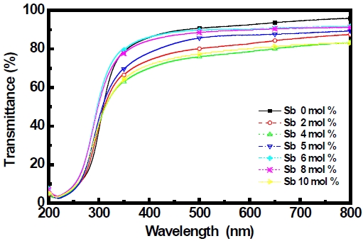
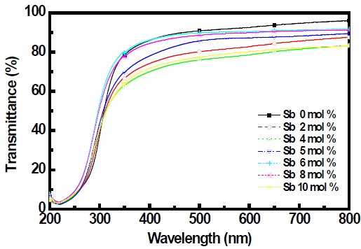
Figure 6 shows the transmittance spectra of ATO thin films as a function of Sb-concentration in low vacuum. In the range of Sbconcentration from 5 to 8 mol%, the average transmittance in the visible range was about 85%, as well as showing a high carrier concentration. However, for 10 mol% of Sb-concentration, the transmittance was decreased by increasing Sb-concentration, and transmittance was about 77%, due to an absorption or impurity scattering, with the increase of the donor.
Sb-doped tin oxide (ATO) thin films on glass substrate have been prepared, by using spin coating with non-alkoxide precursors, and sol-gel derived stock solution. From XRD patterns, randomly oriented Sb-doped SnO2 thin films were observed, while ATO thin film well crystallized at 550℃. The surface morphology of ATO thin films was significantly affected by the annealing atmosphere. Electrical resistivity was decreased by an increase of either Sb concentration or annealing temperature, From Hall measurement, carrier concentration was increased, and mobility was decreased, due to the doping effect. For optical properties, ATO thin films from 5 to 8 mol% of Sb-concentration obtained a good transmittance, and an average transmittance was about 85% in the visible region.