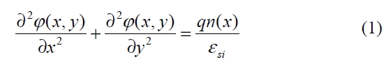
The metal-oxide semiconductor field-effect transistor (MOSFET) scaled down to a sub-10 nm channel length is an essential device for future electronic systems for application to various fields, especially in portable mobile systems. The International Technology Roadmap for Semiconductors (ITRS) shows that CMOS technology will reach fundamental physical limits in the near future [1]. Since short channel effects (SCEs) have happened with serious results for the conventional MOSFET, in order to shrink the device to a sub-10 nm channel length, the multiple gate FET (MugFET) has been developed to improve gate controllability. The symmetric double-gate (DG) MOSFET has been an intensive candidate to remove short channel effects among MugFET. The SCEs, such as threshold voltage roll-off [2], drain-induced barrier lowering [3], subthreshold swing [4], and breakdown voltage [5] have been studied for the DG MOSFET. Relatively few studies have addressed breakdown voltage for the DG MOSFET, and thus further investigation is required to more accurately analyze the SCEs of power DG MOSFETs. The most important problem among SCEs related to the nano scale DG MOSFET is low breakdown voltage. A low breakdown voltage for the DG MOSFET is reasonable since the DG MOSFET has been developed to use the nano scale, and breakdown voltage decreases with the decrease in the channel length as well as the threshold voltage in the n-channel MOSFET. Therefore, investigation of how to control the breakdown voltage of the DG MOSFET is important, especially in the field of power devices. Tiwari et al. [6] have obtained a potential analytical model from Poisson’s equation using the Gaussian function for the doping distribution, and this model has been verified in previous research [7]. In this study, the breakdown voltage model has been derived from Tiwari’s analytical potential model [6] and Fulop’s breakdown condition [8] to investigate the dependence of breakdown voltage on device parameters such as doping concentration and channel length. The shape of the Gaussian function is changed for a projected range and standard projected deviation of doping distribution obtained from the ion implantation process. Therefore, the change in the breakdown voltage has been presented with the parameters of projected range and standard projected deviation.
This paper is organized into four major sections. A 2D analytical potential and breakdown voltage model with Poisson’s equation have been presented in section II. In section III, the breakdown voltages derived from this model have been discussed. The conclusion has been drawn in section IV.
II. POTENTIAL AND BREAKDOWN VOLTAGE MODELS
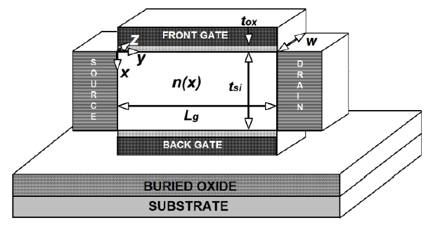
Fig. 1 is the schematic overview diagram of a symmetric DG MOSFET, where
where
where
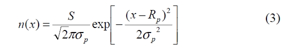
The Gaussian distribution function along the axis of incidence for the implanted impurity profile can be approximated by:
where
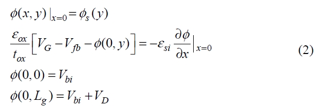
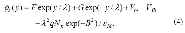
Using the methods proposed by Tiwari et al. [6], the surface potential along the channel derived from Eqs. (1) and (2) is
Refer to the previous paper [7] for
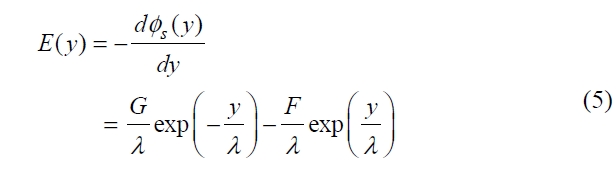
The surface field
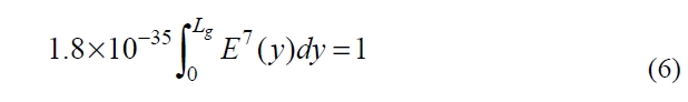
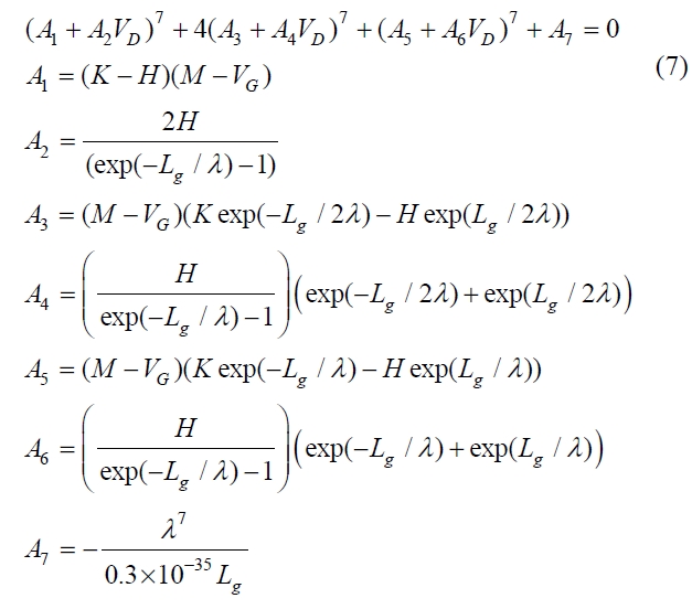
Based on Eqs. (5) and (6), the breakdown voltage is calculated by Simpson’s rule as follows:
Refer to the previous paper [7] for
To investigate the relationship of the breakdown voltage and the shape of the Gaussian function, the breakdown voltage has been calculated for the change in the projected range and standard projected deviation. The
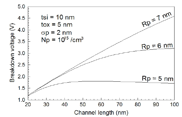
The validity of the analytical surface potential model of Eq. (4) has already been shown in the previous paper [7]. That is to say that this potential model is in good agreement with the numerical simulation. Therefore, this study has reasonably used Eq. (7) to obtain the breakdown voltage. As known in SCEs, the threshold voltage roll-off occurs with the decrement of the channel length and the breakdown voltage is reduced for short channels. Fig. 2 shows the relationship between the breakdown voltage and channel length with a parameter of the projected range. Note the breakdown voltage greatly changes within the projected range as shown in Fig. 2. As shown in Fig. 2, the breakdown volatge increases linearly if the projected range become longer, but it saturates at a critical point if the projected range is shorter. The saturation point becomes short with a decrease in the projected range. In the range of short channel length under sub-20 nm, the breakdown voltage is nearly constant for the change in the projected range, but the difference in the breakdown voltage for the projected range is bigger with an increase in the channel length. If a DG MOSFET needs a large breakdown voltage, the projected range must be large in the process of power DG MOSFET.
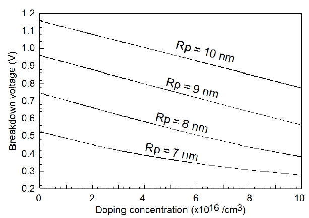
Fig. 3 shows the dependence of breakdown voltage on doping concentration in the case of a channel length of 50 nm, channel thickness of 30 nm, gate oxide thickness of 5 nm, and standard projected deviation of 20 nm. Since the breakdown electric field within the depletion layer increases with increased doping concentration on the lightly doped side of the junction, the breakdown voltage decreases as the doping increases. As shown in Fig. 3, the breakdown voltage is decreased with an increase in the doping concentration in the case of a DG MOSFET. Also, the breakdown voltage increased with the increment of the projected range. Note the rate of increase for the projected range is nearly constant. The breakdown voltage is increased since the increase of the projected range causes a resulting increase in the total dose in the channel in the case that the channel length is longer than the projected range. Compared with Fig. 2, the breakdown voltage is smaller when the channel thickness and standard projected deviation is increased. Consequently, the breakdown voltage increases with the increase in the projected range and the decrease in the standard projected range.
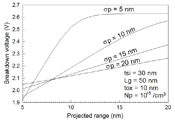
Fig. 4 shows the breakdown voltage for the projected range with a parameter of the standard projected deviation. The device parameters of the DG MOSFET are the same as those of Fig. 3, but only different gate oxide thicknesses such as 10 nm were used. As expected in the previous description, the breakdown voltage increases with the increase in the projected range. The breakdown voltage is linearly increasing in the range of the standard projected deviation of above 10 nm, but it is saturated at the critical point of the standard projected deviation in the range of the smaller standard projected deviation. Compared with Fig. 3, note the larger breakdown voltage derived from the large gate oxide thickness under the same conditions of the other parameters. The smaller the standard projected deviation is, the larger the breakdown voltage becomes in the high projected range. However, the larger the standard projected deviation is, the larger the breakdown voltage becomes in the low projected range, as shown in Fig. 4.
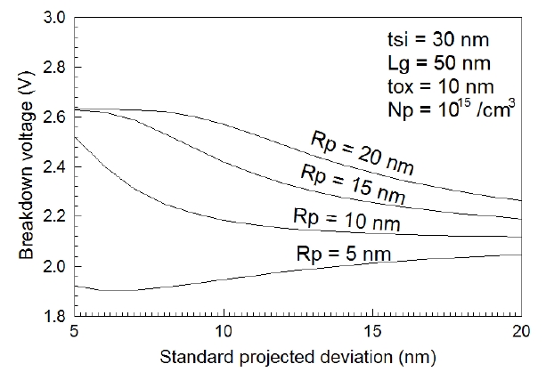
Fig. 5 shows the breakdown voltage for the standard projected deviation with a parameter of the projected range. The device parameters used are the same as those of Fig. 4. The decrease and increase of breakdown voltage for the standard projected deviation depend on the values of the projected range. As shown in Fig. 5, the breakdown voltage is increasing with the increase in the standard projected deviation in the lower projected range such as below 5 nm, but it is decreasing with an increase in the standard projected deviation in the relatively higher projected range. Also, the breakdown voltage has been greatly influenced by the projected range in the lower standard projected deviation, but the larger the standard projected deviation is, the smaller the influence on the projected range for the breakdown voltage becomes. The breakdown voltage is ultimately saturated with an increase in the standard projected deviation regardless of the projected range.
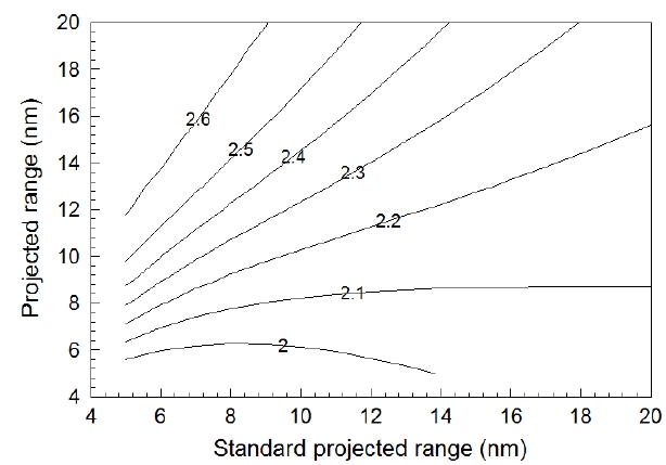
To investigate the relationship between the breakdown voltage of the projected range and the standard projected deviation in detail, the contours are plotted in Fig. 6 under conditions of device geometry and doping concentration such as those of Fig. 5.
Like Figs. 4 and 5, Fig. 6 shows that the breakdown voltage is increasing with the increase in the projected range and decrease in the standard projected deviation. However, in the lower region of the projected range, the contour trend of the breakdown voltage is decreased with the decrease in the standard projected deviation. Note the contours are nearly linear above the breakdown voltage of 2.2 V under the chosen conditions. The changing rate of the breakdown voltage is larger in the region of low projected range and standard projected deviation, but it is smaller in the region of a large projected range and standard projected deviation. Therefore, to fabricate the DG MOSFET with a low projected range and standard projected deviation, the projected range and standard projected deviation must be controlled carefully.
This study has presented the analysis of breakdown voltage for the double-gate MOSFET based on the shape of the Gaussian function used to solve Poisson’s equation. The lowering of the breakdown voltage is one of the very important short channel effects along with threshold voltage roll-off, degradation of subthreshold swings, and so forth. This study has presented analytical potential distribution and breakdown voltage models derived from Poisson’s equation and Fulop’s avalanche breakdown condition to analyze the breakdown voltage of the DG MOSFET for shapes of Gaussian doping distribution, observing the changes in the breakdown voltage for channel length, doping concentration, and gate oxide thickness. The breakdown voltage has been reduced for short channel length due to SCEs such as threshold voltage roll-off. Also, the breakdown voltage is decreased with the increase in the doping concentration in the case of the DG MOSFET as well as the conventional MOSFET due to an increase in the breakdown electric field. Additionally, the breakdown voltage increased with the increase in the projected range and decrease in the standard projected deviation. Consequently, the double-gate MOSFET has to be carefully designed and fabricated since the breakdown voltage is greatly changed for shapes of the Gaussian function.