In the past several years, graphene, a one-atom-thick two-dimensional (2D) sheet of sp2-hybridized carbon atoms, has attracted enormous interest by opening up possibilities for advanced nanoelectronic devices, due to its unique physical properties, such as quantum electronic transport, a controllable band gap, outstanding high mobility, and high flexibility [1-4]. In 2004, the first isolation and investigation of single layer graphene was reported by Geim and Novolselov [3] using a mechanical exfoliation method, which is a time consuming process, and cannot be scaled for large-area uniform graphene. In 2009 chemical vapor deposition (CVD) methods with metal catalysts on Ni or Cu catalyst metals were developed for the growth of large-area uniform graphene films [5-8]. Although the CVD grown graphenes have been used in various application areas, we should address some obstacles, such as catalyst material, growth conditions, etching problems, transfer and non-ideal properties for the realization of graphene devices.
Among these, we focused on the etching problem, which is expected to affect the properties of CVD-grown graphene on a Ni catalytic layer. Usually, an FeCl3 solution was used to etch the catalytic Ni layer for segregating graphene. However, through elemental analysis, using the X-ray photoelectron spectroscopy (XPS), we observed the residue of Fe containing a small amount of Cl after etching of the catalytic layer. This residue can affect the material properties of the isolated graphene. In this work we provide an alternative etching solution by introducing acidic etching solutions and their combinations to remove this residue, and present the characterization of CVD grown graphene with various etchants for a Ni catalytic layer.
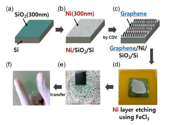
In this work, we used CVD grown graphene on a Ni catalyst for identifying the effect of residue on the properties of graphene. The schematic illustration of the growth and transfer process for CVD-grown graphene is shown in Fig. 1. We prepared an SiO2 (300 nm)/Si substrate and deposited 300 nm Ni layer on the substrate as shown in Figs. 1a and b. For the growth of graphene films we exposed the Ni/SiO2/Si substrate to reaction gas mixture atmosphere (Ar : H2 : CH4) for a few minutes at 1000℃ . Graphene films were grown on the in a quartz tube furnace under (Fig. 1c) [9]. After cooling the sample to room temperature, the Ni catalytic layer was etched to release an isolated graphene film from the SiO2/Si substrate using a FeCl3 (iron III chloride) solution as in Fig. 1d. Then, the graphene film was floated on DI-water and rinsed to remove contaminating residues as in Fig. 1e. Finally the rinsed graphene film was transferred to a target substrate and baked at 60~90℃ for a few minutes to increase the adhesion between graphene film and the target substrate.
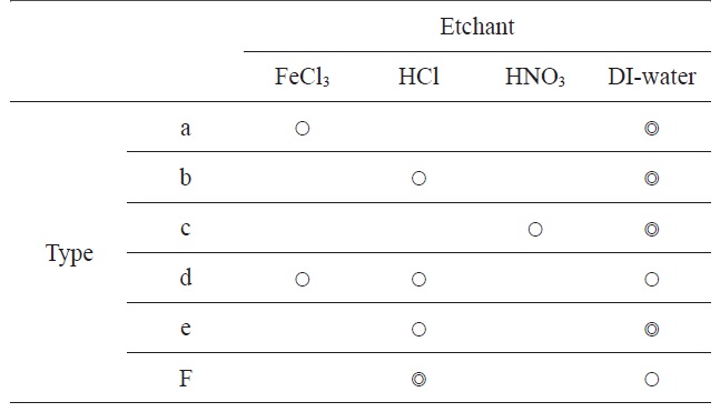
[Table 1.] Combination etchant types

Combination etchant types
In this work we used aqueous FeCl3 solution as an etchant to remove the nickel layer. The etching reaction can be represented by the following chemical reaction,
2Fe3+(aq)+ Ni(s) → 2Fe2+(aq) + Ni2+(aq).
After the etching and rinsing process, some residues of the chemical reaction were identified on the graphene surface. To remove the residue, we choose several etchants and combined etchants. As summarized in Table 1, we used three kinds of etchant chemicals, FeCl3, HCl, and HNO3, and combined 6 process types. The concentration of FeCl3, HCl, and HNO3 solutions were 1 M, 5.5 M, and 5.5 M, respectively. The concentration of acid solutions, HCl or HNO3, should be higher than the FeCl3 solution because the etch rates of acid solutions for Ni layer were substantially low. Moreover we found some problems in the etching processes using acid-only solutions, in which thin oxide films formed on the Ni surface, and then some hydrogen bubbles made defects on the resulting graphene surfaces. Therefore, in this work, we measured and analyzed the residue of etching processes for three process types, type a (FeCl3+ DI-water + DI-water), type d (FeCl3 + HCl + DI-water) and type f (HCl + HCl+ DI-water).
Graphene films were deposited on Ni/SiO2/Si substrates in CH4 (50 sccm), H2 (50 sccm), and Ar (200 sccm) ambient atmo-
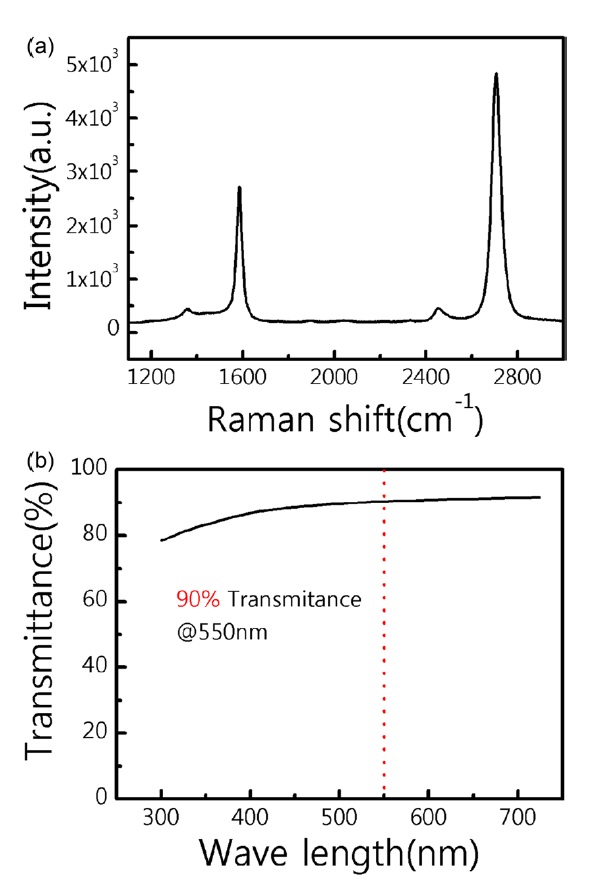
spheres by thermal CVD method. The graphene films consisted of ~4 layers with a thickness of ~2 nm. As shown in Fig. 2a, the Raman spectrum of a transferred graphene film on SiO2/Si substrate was measured by Raman microscope (CRM 200 Witech, 532 nm laser wavelength). The Raman measurement was performed using a 514-nm excitation source at a laser power of 20 mW. Major Raman peaks of graphene were observed in the D band (~1350 cm-1), G band (~1580 cm-1), and 2D band (~2700 cm-1). The optical transmittance and electrical properties (sheet resistance and hall mobility) of graphene films were measured
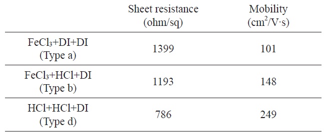
[Table 2.] Sheet resistance and mobility of graphene films in terms of various etching process types

Sheet resistance and mobility of graphene films in terms of various etching process types
by an UV spectrometer and a Hall measurement, respectively. The transmittance of graphene film was 90% at 550 nm, which corresponded to 4 layers of graphene, because an individual graphene layer absorbs ~2.3% of visible light [9]. These Raman spectra and transmittance were reproducible for 6 etching processes.
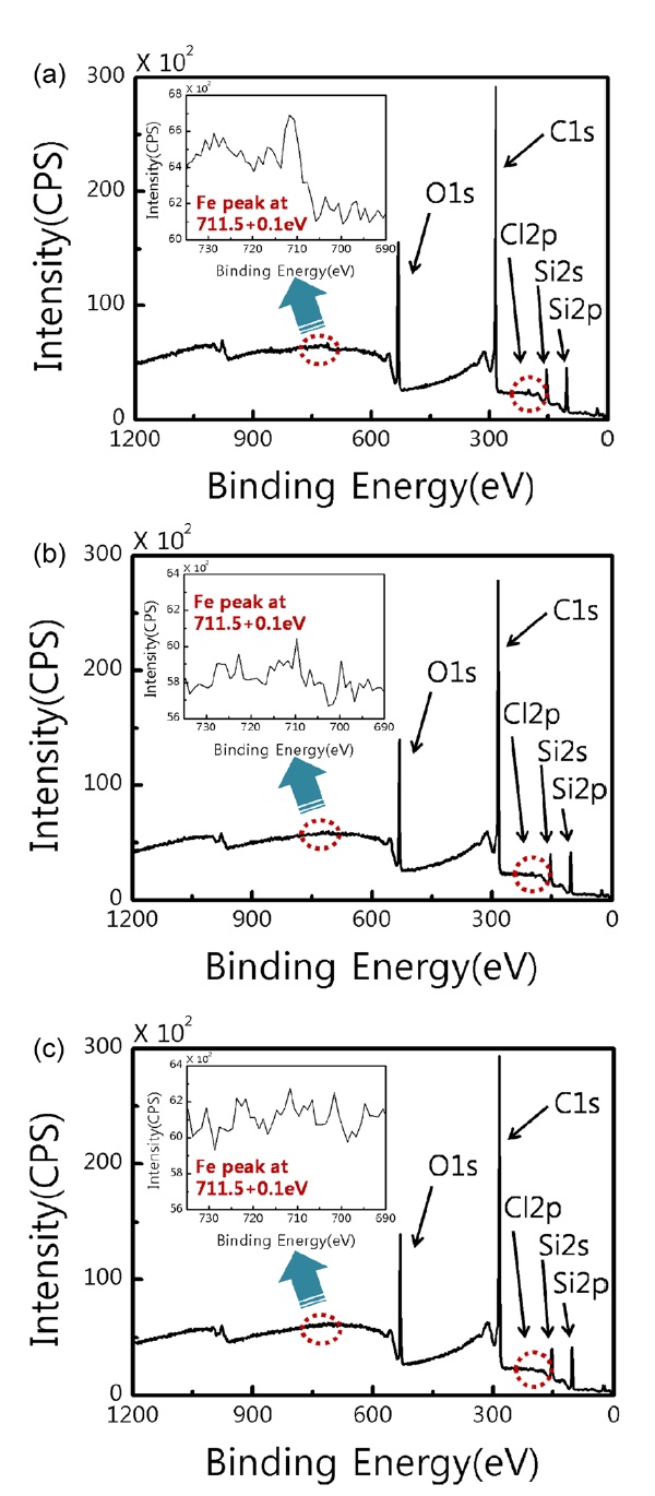
We used the X-ray photoelectron spectroscopy (XPS) to analyze the nature of residues after each etching process. Fig. 3 shows XPS spectra of graphene films from three different etching processes, type a, type d, and type f. For three different graphene films we compared the existence and intensity of Fe and Cl peaks. As shown in Fig. 3a (type a), an Fe peak and Cl peak were found at 711 eV and at 198 eV respectively. The type d (Fig. 3b) still had an Fe and Cl peak, but the intensity and full width at half maximum of the Fe peak at 711 eV was decreased, compared with type a. This means that the Fe residue can be removed by an acid etchant like HCl. Fig. 3c shows the analysis of the graphene surface using the type f. As we expected, this sample did not show Fe and Cl peaks, and only had O and C peaks.
The electrical properties of graphene films were characterized by the sheet resistance and hall mobility. The graphene film produced from the standard etching process, type a, showed the sheet resistance of ~1399 ± 100 Ω/sq and hall mobility ~100 cm2/Vs, respectively. But the sheet resistance and mobility of graphene were changed with the amount of etching process residue. In case of type d (FeCl3 + HCl + DI-water), sheet resistance decreased 14% and mobility increased 46% compared with type a. For type f (HCl + HCl + DI-water) etching process, the sheet resistance decreased 43% and the mobility increased 246% compared with the type a graphene film (Table 2). From these results, we could propose that the residue materials affect the electrical properties of graphene and the etchants should be carefully selected.
In conclusion, we investigated the effect of etchants for the metal catalyst in terms of the characteristics of the resulting graphene films. We found the residue of FeCl3 etchant substantially degraded the electrical properties, the sheet resistance and the mobility of graphene films. The residues on graphene films were identified as Fe and Cl by using the XPS, and the effect of the residues on optical and electrical properties of graphene were measured by Raman, UV spectrometers, and hall measurement. We can propose that the residue materials affect the electrical properties of graphene and the etchants should be carefully selected.