Since mono-layer graphene was isolated by Geim and Novoselov, numerous studies focused on various applications of graphene have been carried out in efforts to realize graphene-based devices. In this regard, the synthesis of large-area, high-quality graphene is a fundamental requirement. To date, epitaxial growth on SiC [1-3], chemical vapor deposition (CVD) methods on catalytic metal substrates [4-9], and chemical reduction of graphite oxide [10-13] have been widely studied for large-scale graphene synthesis. Notably, Hong and his colleagues [14] recently showed that the CVD method enables the synthesis of 30-inch wide high quality graphene. However, due to imperfect crystallinity and inherent defects, these synthetic graphene films have lower carrier mobility than mechanically cleaved graphene. For the measuring of the inherent defects in CVD grown graphene layers, Raman spectroscopy, atomic force microscopy (AFM), scanning electron microscopy (SEM), and tunneling electron microscopy are typically utilized. However, these methods are not suitable for the quantitative analysis of defects in graphene over a large area. Selective electrochemical deposition (SED), on the other hand, is a possible solution for efficient and quantitative measurement of the defect densities in synthetic graphene layers. Because the defect sites of graphene are more reactive than the pristine sp2 bonded graphene lattice, defect sites can be decorated with high selectivity [15-21].
Here, we carried out SED of Au nanoparticles on defect sites on CVD grown graphene layers, and the origin of the defects is suggested on the basis of the results.
2.1. Graphene synthesis and sample preparation
The graphene layer was synthesized on the Cu surface by the CVD process using radio-
frequency (RF) plasma. A 300 nm thick Cu film deposited on top of a Si wafer with a 300 nm thick SiO2 layer was inserted in an inductively coupled plasma CVD system. After ramping up temperature to 725℃ under Ar ambient at 50 mtorr, the sample was treated by H2 plasma with a gas flow rate of 40 sccm and RF plasma power of 50 W for 2 min. A gas mixture of Ar and C2H2 (Ar:C2H2 = 40:1 sccm) was then flowed into the chamber with 150 W RF plasma for the graphene synthesis. The graphene layer synthesized on the Cu surface was finally transferred onto the SiO2 (300 nm)/Si using a poly(methyl methacrylate) supporting layer and wet etching of the metal film.
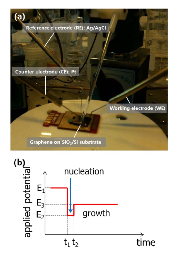
To selectively decorate Au nanoparticles on graphene, we used electrochemical deposition. Employing a multi-potential system, we controlled both the nanoparticle size and packing density. A droplet of HAuCl4 in 100 mM KCl (supporting electrolyte) was placed on the device and transferred graphene was used as a working electrode. A reduction potential was then applied with respect to an Ag|AgCl|KCl (3M) reference electrode with current monitoring using a Pt counter-electrode.
2.3. SEM and energy dispersive X-ray spectroscopy analysis
The Au particle decorated graphene samples were observed by a field-emission SEM/energy dispersive X-ray spectroscopy
(EDAX) system (FEI Sirion SEM with an EDAX, The Netherlands). Prior to observation, the samples were placed on a metal stub with double sided carbon adhesive tape. The scanning energy for the EDAX analysis ranged from 0 to 4.75 KeV.
The measurement configuration and engineered potential pulse are shown in Fig. 1. A drop of 50 μM HAuCl4 solution was placed onto the transferred graphene. Deposition of Au nanopar-
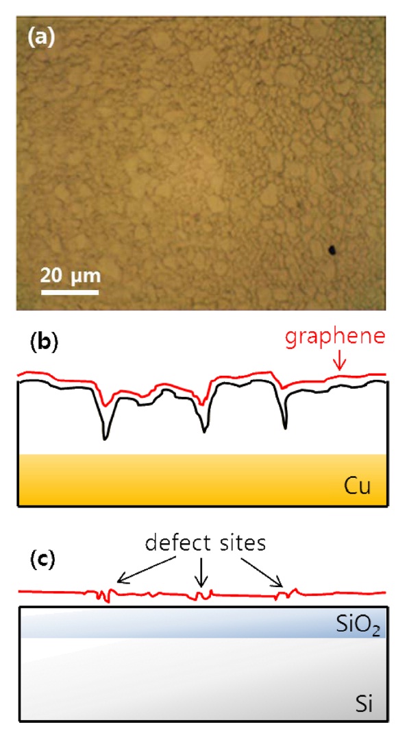
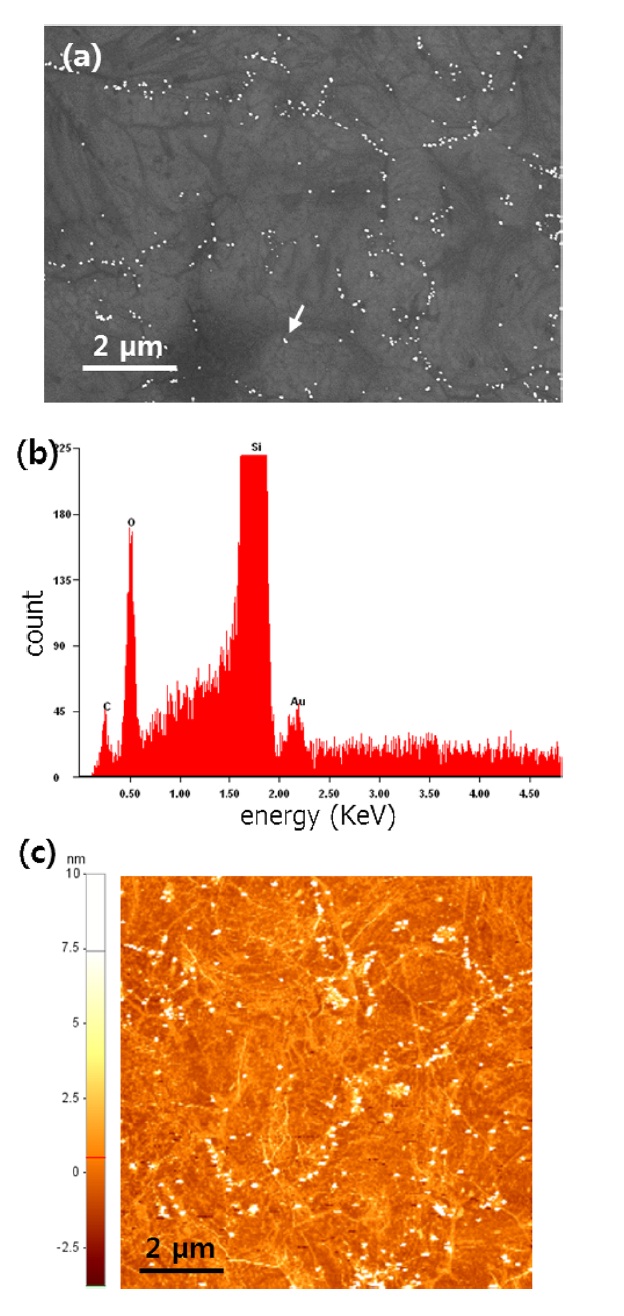
ticles entailed three steps: protection, nucleation, and growth. The first step for the protected Au particles was applied at 1 V for 3 s. Following the first step, a pulse with E2 = -0.6 V for 50 ms initiates nucleation at the prepared sites. Growth was continued at E3 = 0.6 V for 1 s. We typically obtained roughly 30-nmsize Au nanoparticles using the above method. An SEM image of the Au nanoparticle decorated graphene surface is presented in Fig. 2a. As reported earlier, wrinkles caused by different coefficients of thermal expansion between graphene and the Cu substrate and mechanical stress induced during layer transfer are observed over the entire graphene surface [8,9]. The shape and density of these wrinkles are more clearly shown in the AFM image (Fig. 2c). After SED by an engineered potential pulse, Au nanoparticles are situated in specific positions, as shown in Figs. 2a and c. The EDAX spectrum for a white particle (white arrow) in the SEM image (Fig. 2b) exhibits a clear Au peak, implying the nucleation and growth of Au nanoparticles. Even though there are numerous wrinkles over the whole graphene surface, as shown in the SEM and AFM images, most Au nanoparticles are not located on these defects but instead form a specific shape that resembles a grain boundary of the Cu substrate shown in Fig. 3a. The Cu surface is inevitably agglomerated and roughened during the graphene synthesis because of the high temperature annealing, an essential process for high quality synthesis of high quality graphene layers. Thus, as shown in Fig. 3b, the graphene layers are synthesized along the highly roughened Cu surface. During the layer transfer of synthetic graphene onto the flat SiO2/Si substrate, this uneven graphene layer is folded, and defect sites are formed on the graphene layer (Fig. 3c). Consequently, the higher reaction energy of these defects caused by the rough surface of Cu attracts the Au nanoparticles.
In this work, we have quantitatively investigated the defects on large size, high quality graphene layers grown by the CVD method via SED of Au nanoparticles. By adjusting the potential applied to the graphene, selective deposition of Au nanoparticles on specific defect sites was achieved. Comparing the positions of defect sites and the Cu grain boundary, it is confirmed that most defect sites are caused by the unevenly synthesized graphene along the rough Cu surface.