Zinc oxide (ZnO) has gained considerable attention as a material for short-wavelength optoelectronic devices, such as photodetectors,light-emitting diodes, and laser diodes, because of its wide band gap of 3.37 eV and large excitation binding energy of 60 MeV at room temperature [1,2]. Normally, undoped ZnO exhibits n-type conductivity.
The implementation of
compensation for the acceptors). Even though many research efforts have been made to prepare N-doped
Dielectric barrier discharge (DBD) is a kind of non-equilibrium, non-stationary discharge method. Recently, production of N-doped ZnO thin films has been reported using DBD as an assisted plasma-activation source in pulsed laser deposition (PLD) [25]. In addition, it has been confirmed that an activated source in a DBD system is a more effective way to realize doping in ZnO, which depends directly on the supply of ionized dopants.
In this study, N-doped ZnO thin films have been grown on a sapphire substrate by DBD in PLD. This approach is critically important in the diversification of tools to achieve reliable and effective N-doping of ZnO. The structural and optical properties of the N-doped ZnO thin films are examined using X-ray photoelectron spectroscopy (XPS) and photoluminescence (PL) to verify the N-doping.
N-doped ZnO thin films were grown at room temperature by a combined DBD-PLD method in which the N doping source was generated under normal PLD process conditions. During growth, the background gas pressure was maintained at 350 mTorr. A caxis-polished sapphire was used as a substrate. For laser ablation in PLD, an Nd:YAG laser with a frequency of 5 Hz and an energy density of 1 J/cm2 was used. The thickness of the thin films was measured as approximately 300 nm. Thermal annealing was carried out at 800℃ for 15 minutes under oxygen ambient. The structural property of the samples was investigated by X-ray diffraction using an Ni-filtered Cu K source, and the binding structural properties were analyzed with XPS. The optical properties were characterized by PL with a He-Cd laser of excitation wavelength 325 nm and power 20 MW serving as a light source.
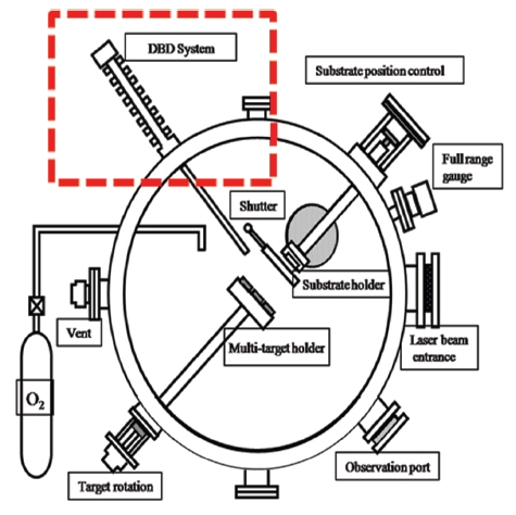
Figure 1 shows a schematic diagram of the DBD in the PLD equipment that is designed to generate and provide the active N source. A quartz tube with a relatively high dielectric constant (εr = 3.9) was used as a dielectric barrier material in the discharge zone. A tungsten (W) discharge electrode was used as a power
electrode at the center of the quartz tube, and an aluminum radiator was used as a ground on the outside of the quartz. To generate a microdischarge between the power electrode (W) and the inner wall of the quartz tube, an alternating current (AC) was applied between the W rod and the Al electrode. For effective removal of the heat originating in the microdischarges, a round aluminum shape with a large number of fins was added. A cooling water system with a cooling fan was also set up in the region of the aluminum radiator. AC power was supplied at the stainless tube. The end of the quartz tube was connected to the N inlet.When high-purity N gas flowed in the discharge gap through the four holes in the stainless tube, a micropinning discharge between the electrodes dissociated the N2 molecules and produced active N atoms which could be used as the N source for doping. The formation of atomic N could be confirmed by observing an afterglow of yellowish-orange light. The AC electric power and frequency required for the continuous discharge reaction were determined by the gap between the dielectric barrier and the electrode, the radio frequency power, and the gas pressure. The system was equipped with an impedance-matching device with a serial inductor to keep it within the 200-300 kHz frequency range. Impedance matching was achieved by tuning the frequency at constant capacitance (C) and reactance (L). With the matching network, an root mean square voltage between power and ground electrodes of approximately 3 kV could be obtained. Active N species from the discharge zone were supplied to the front part of the PLD chamber
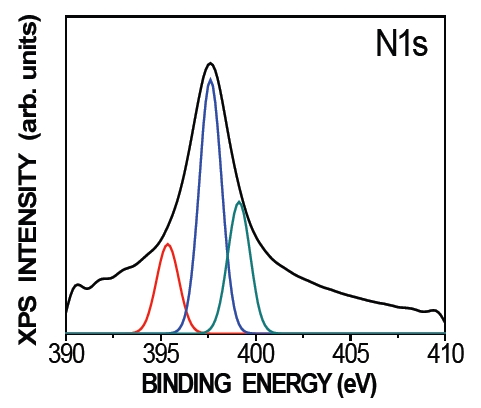
To understand the origin of defect compensation, XPS was used to identify the chemical state of the N atoms in N-doped ZnO.
Theory predicts that N can be incorporated into ZnO in at least two different states. N-atom substitution into the oxygen site of ZnO (NO) is a desired acceptor [26], and (N2)O is a N2 molecule occupying a position on the oxygen sublattice as a shallow double donor. Figure 2 illustrates an N 1s narrow-scan spectrum for N-doped ZnO thin films grown on a sapphire substrate by DBD in PLD. One peak with a maximum at approximately 397.84 eV can be observed, which corresponds to the N 1s core level. The peak of the N 1s core level can be fitted into one Gaussian peak by deducting the base line, which indicates that only one chemical-bonding state of N exists in N-doped ZnO thin films. The N 1s peak centered at 398 eV can generally be attributed to N-Zn bonding [16,26]. By fitting an experimental line profile, three deconvoluted peaks centered at 395.35, 397.64, and 399.07 eV were identified. The peak at 395.35 eV is an assigned value of atomic β-N binding energy [27]. The higher binding energy spec-
trum centered at 397.64 and 399.07 eV is associated with N-Zn and N-O bonding. Note also that the (N2)O chemical state does not exist in these ZnO thin films because the peak at the reported (N2)O binding energy of 404 eV is absent [28]. Therefore, it can be concluded that the incorporated N in the films exists as NO rather than (N2)O. The N-Zn bond dominates in the XPS spectrum for the N-doped sample, which confirms that the N mainly forms an NO state in ZnO.
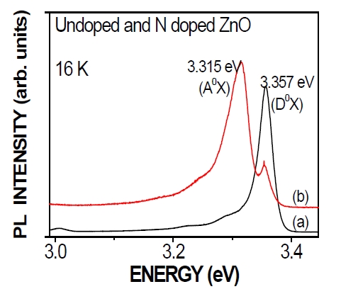
Figure 3 shows PL spectra comparing the annealed N-doped ZnO films and undoped ZnO films. Undoped ZnO films showed dominant donor-bounded excitation (D0X) peaks, whereas N-doped ZnO films clearly showed acceptor-bounded excitation (A0X) peaks. For the undoped ZnO films, a dominant near-bandedge emission peak was observed at 3.357 eV. This emission is associated with a donor-bound excitation state (D0X), which apparently originates from the hydrogen-bound excitation state denoted as I4 in the literature [29]. The low-temperature PL spectrum of the N-doped ZnO films significantly differs from that of undoped ZnO films by exhibiting two dominant broad peaks centered at 3.315 and 3.357 eV. Many studies indicate that this peak at 3.315 eV can be attributed to an A0X emission caused by an N acceptor [30].
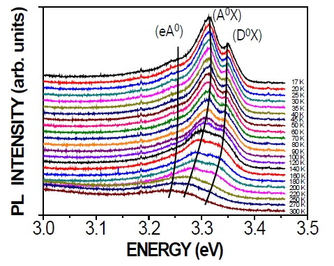
Figure 4 shows the temperature-dependent PL spectra of N-doped ZnO measured from 16 K to 300 K. The PL spectra of ZnO are focused mainly at the near band edge. As shown in Fig. 4, there are three peaks, (D0X), (A0X), and (eA0), at the low-temperature end. It has been found that these three peaks shift toward the lower-energy side with increasing temperature, a phenomenon caused by thermal activation of carriers.
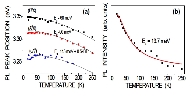
Figure 5(a) shows the peak-position behaviors of the (D0X), (A0X), and free-electron-neutral-acceptor transitions (eA0) based on temperature-dependent PL measurement, as shown in Fig. 4. The temperature-dependent band gap can be described by the Varshni equation according to [31] as:
where Eg(T) is the temperature-dependent band-gap energy, α is related to the excitation-average photon interaction, and β is closely related to the Debye temperature. The solid curves in Fig.5(a) are least-squares fits made with the fitting parameters as noted. From this analysis, the (D0X) and (A0X) emission binding energies can be estimated as 60 MeV and 90 MeV respectively, as shown in Fig.5 (a).
For the (eA0) emission, the temperature dependence of the peak position can be well described according to [32] as,
where EA is the acceptor energy level and kB is the Boltzmann constant. The curve fitted to the data gives an acceptor level of 145 MeV, as shown in Fig.5 (a). This value agrees with the reported values for N-doped ZnO, such as the 140 MeV reported by Ye et al. [33]. The good match obtained between the experimental values and the fitted curves confirms the assignment of the (eA0) transitions in the present research.
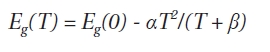
Figure 5(b) shows the integrated intensity of the (A0X) emission as a function of temperature for the annealed N-doped ZnO sample. The observed overall temperature-quenching behavior can be well described by the equation:
where I0 is the emission intensity at zero temperature, A is a parameter, and Ea is the activation energy in the thermalquenching process. The good fits (solid curves) yielded an Ea value of 13.7 MeV. Using the Haynes rule, Ea/EA ~0.1 for a ZnO material system, and the acceptor binding energy EA can be estimated as 0.137 eV. This result is in good agreement with the calculated EA value from measurements.
In conclusion, N-doped ZnO thin films were deposited on caxis-polished sapphire substrates using DBD in a PLD system. One peak with a maximum at approximately 398 eV could be observed, which corresponds to the N 1s core level. It was proved that the N was successfully incorporated into the oxygen site in ZnO films. In addition, the annealed N-doped ZnO films clearly showed (A0X) peaks using low-temperature PL measurements, and their acceptor-binding energies showed a good match between the experimental data and the calculated fitted values, a match which was further demonstrated by acceptor-related transitions such as (A0X) and (eA0). Through this work, it is demonstrated that DBD in a PLD system can be used for