Since the invention of Fullerene C60 by Kroto in 1985[1], C60 and its derivatives have been used in various applications, including solar cells [2], light emitting diodes [3] and hydrogen storage [4], due to their unique structure and properties. Pure C60 films are semiconductor materials possessing a band-gap of 1.5 eV and an electrical resistivity of 103-108 Ω· cm at room temperature. In order to improve the conductivity of C60 films, boron atoms can be introduced into the C60 lattices. The preparation of boron doped C60 films was firstly reported by Zou et al. [5,6], however no applications were proposed in their works.
In this study, the boron doped C60 films were prepared by the thermal evaporation of C60 powder using argon plasma treatment. The electrochemical application of the film is then introduced. Specifically, the boron doped C60 film was used as a coating layer for silicon anodes in lithium secondary batteries. Furthermore, the effect of argon plasma treatment on the structural and electrochemical characteristics of the coated silicon electrodes was also investigated.
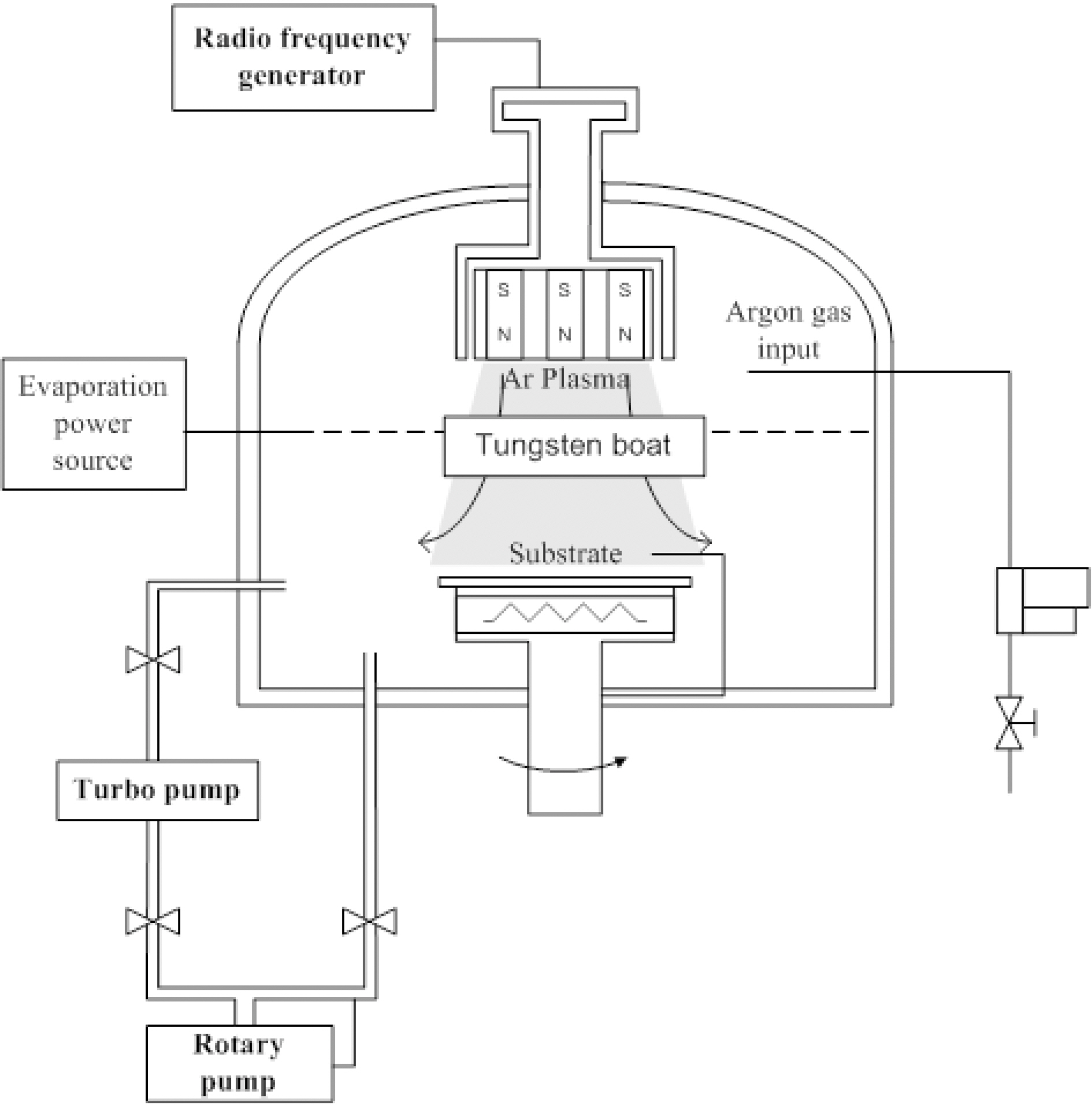
For the deposition of the thin film, C60 powder was loaded into a tungsten boat, as depicted in Fig. 1. The substrate was located on a steel holder and placed about 10 cm from the boat. The substrates were a silicon wafer for the structural
studies and a silicon film on Cu foil for the electrochemical tests. Firstly, the pressure inside the chamber was reduced to a base pressure of 10-5Torr using a rotary pump. After that, a mixture of argon and diborane (B2H6) was entered into the chamber with a flow rate of 30 sccm (standard cubic centimeters) to reach a working pressure of 2.5.10-2Torr. The flow rate was adjusted by a mass flow controller (MFC). Then, the radio-frequency generator was activated to generate the argon plasma. At the same time, the C60 powder was evaporated by thermal heat input. The resulting C60 vapor in the argon plasma environment was deposited in the form of a thin film on the substrate and the boron atoms were inserted into the fullerene film lattices. The substrate temperature was set at 150℃ and a plasma power of 100W was used during the deposition process. For the comparison study, a pristine C60 film was also deposited by the thermal evaporation of C60 powder. The evaporation was done under the same conditions as that used for the B: C60 film without the argon plasma treatment.
The surface morphology and structure of the thin films were examined by scanning electron microscope (SEM), Fourier transform infra red spectroscopy (FTIR, Nicolet Almega XR, Thermo Electron Corporation) and x-ray photo electron spectroscopy (XPS, VG Scientific ESCALAB 200R). The electrochemical characteristics were studied by cyclic voltammetry (CV) measurements at a scan rate of 0.005 mVs-1 within a cut-off voltage range of 0~3 V. For the CV tests, half cells were then fabricated in a dry room. The half-cells were fabricated by sandwiching a polyethylene (PE) separator between the B:C60 coated Si film electrode (as the working electrode) and Li metal (as the counter electrode). The half-cell (2 cm×2 cm) was then sealed in an aluminized polyethylene bag. The electrolyte was 1 M LiPF6 in a mixture of ethylene carbonate (EC), ethyl methyl carbonate (EMC) and dimethyl carbonate (DMC) (1 : 1 : 1 by volume).
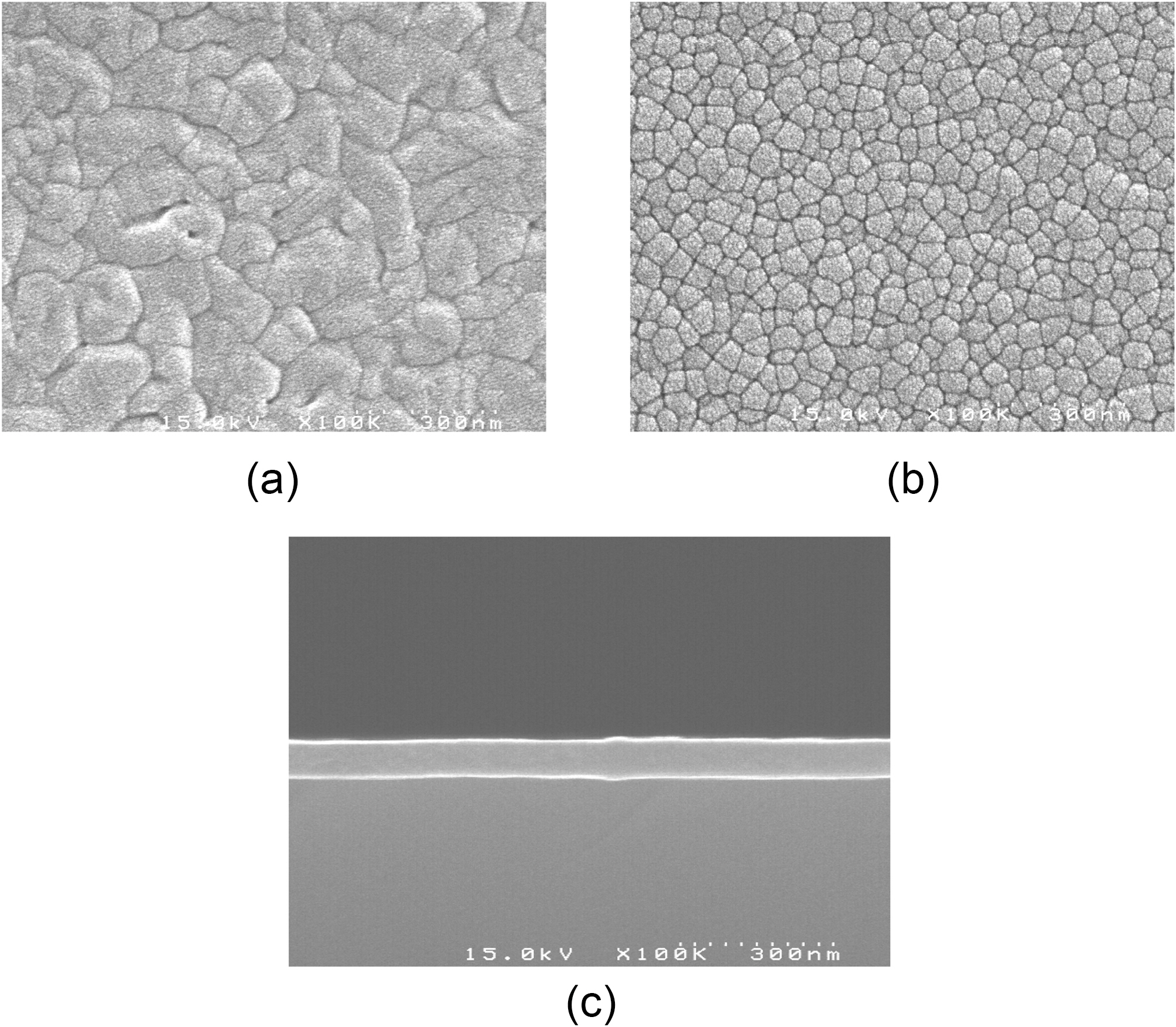
Fig. 2 a shows the SEM photographs of the pristine C60 film synthesized by the thermal evaporation technique without argon plasma treatment. From the surface view, it can be seen that the film consists of many grains with different sizes, due to the evaporation of the C60 powder. In contrast, the B:C60 film shows a smaller grain size with a more uniform shape, as depicted in Fig. 2 b. It seems that the insertion of the boron atoms assisted by the argon plasma treatment during the deposition of the film contributes to the smaller grain size of the B:C60 film. From the cross-sectional SEM image in Fig. 2 c, the thickness of the B:C60 film is estimated to be 100 nm.
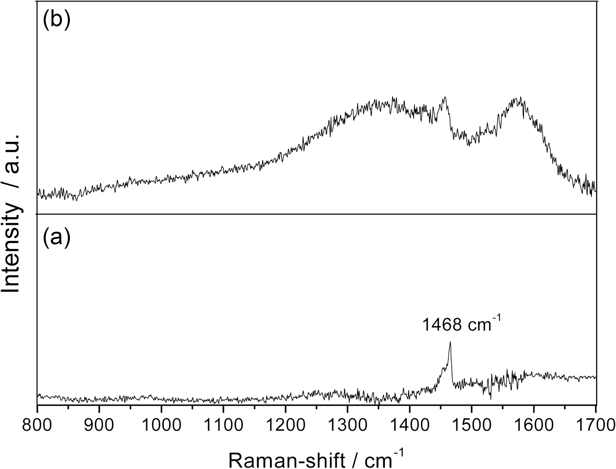
Fig. 3 shows the Raman spectra of the pristine C60 film deposited by the evaporation technique without argon
plasma treatment and the B:C60 film synthesized with argon plasma treatment. It can be seen that a strong peak at Raman shift of 1468 cm-1, known as the pentagonal pinch mode, is observed in the case of pristine C60 film [7,8]. However, this pentagonal pinch mode are gradually separated and broadened but its existence is still recognized in the case of B:C60 films. This broadened peak in the vicinity of pentagonal pinch is the main indication of the typical fullerene C60 structure, which can not be found in other structure of carbon such as graphite, diamond or carbon nano-tubes [9-12].
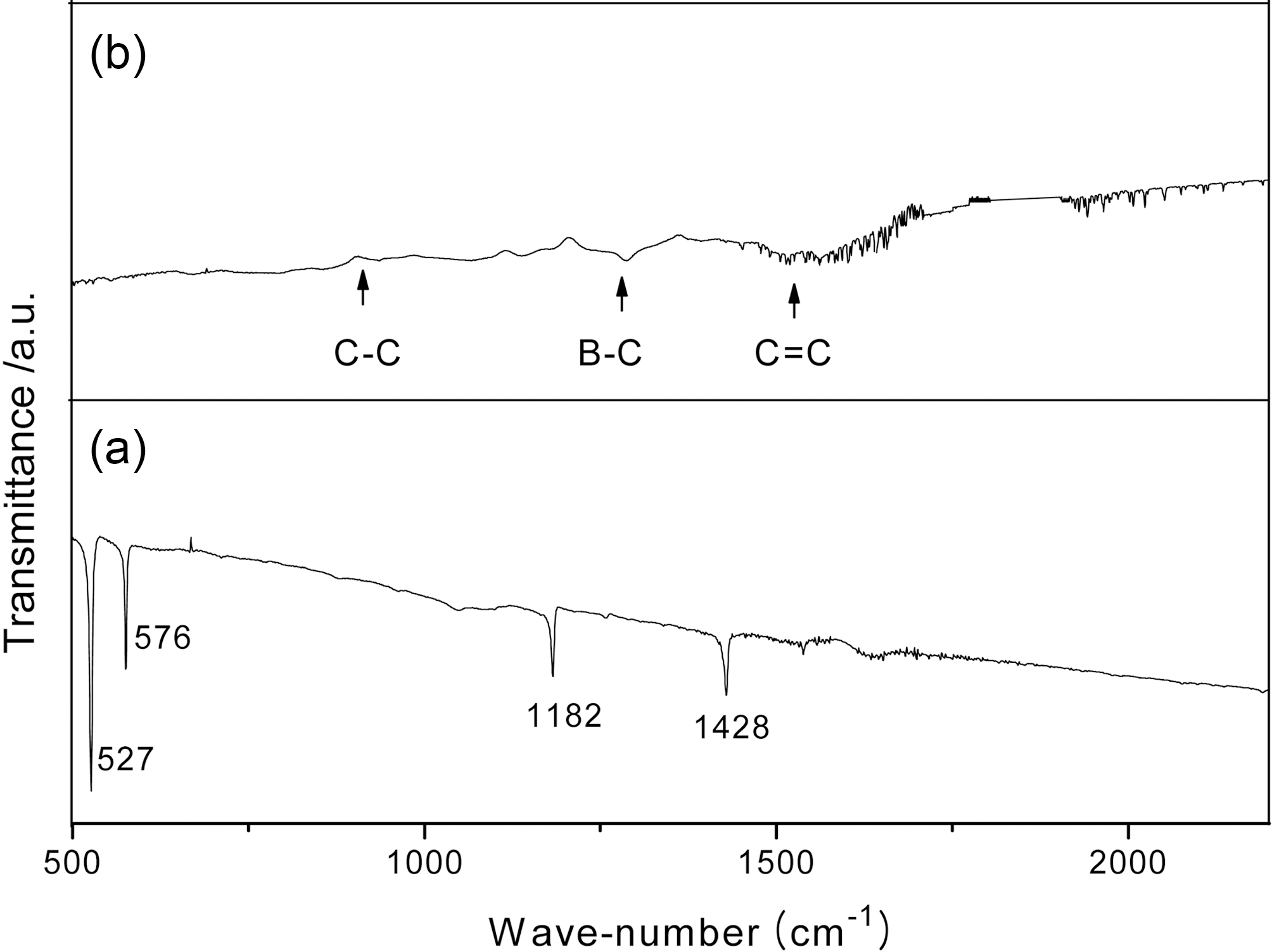
Fig. 4 shows the FTIR spectra of the pristine C60 film deposited by the evaporation technique without argon
plasma treatment and the B:C60 film synthesized with argon plasma treatment. In the case of the pristine C60 film, there are four dominant peaks detected at wave-numbers of 511, 527, 1182 and 1428 cm-1. However, these four peaks are not found in the spectrum of the B:C60 film, in which many new peaks related to the vibration of the bonding states of C-C, C=C and B-C are observed. Therefore, the bonding between boron and carbon in the B:C60 film can be detected, due to the presence of the weak vibration of the B-C bond located at a wave-number of 1260 cm-1.
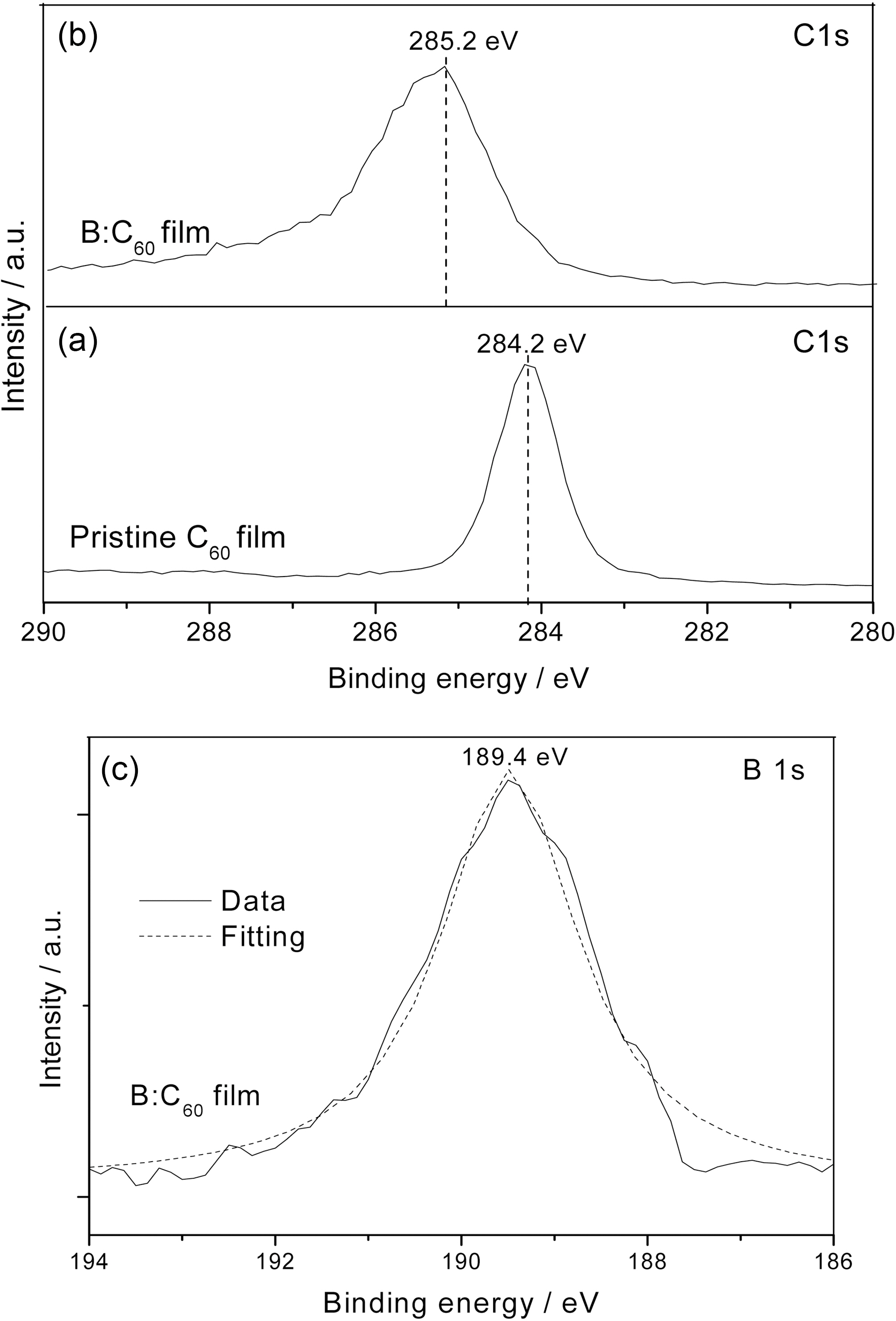
Fig. 5a shows the C 1s XPS spectra of the pristine C60 and B:C60 films. The C 1s binding energies of the pristine C60 and B:C60 films are determined as to be 284.2 and 285.2 eV, respectively. The binding energy in the B:C60 film is shifted to a higher value, due to the presence of stronger bonding between the carbon molecules. The full width at half maximum (FWHM) of the C 1s peak for the B:C60 films is determined to be 1.58 eV. This value is obviously larger than that of the pristine form (0.96 eV). This higher FWHM value and broader spectrum of the B:C60 films indicates that the linking among the fullerene molecules takes place during the deposition process. The presence of boron atoms in the fullerene lattices is evidenced by the B 1s XPS spectra of the B:C60 film, as shown in Fig. 5 b. The peak centered at 189.4 eV is an indication of the bonding between boron and carbon in the fullerene film, which is consistent with the spectra found in the literature [13,14].
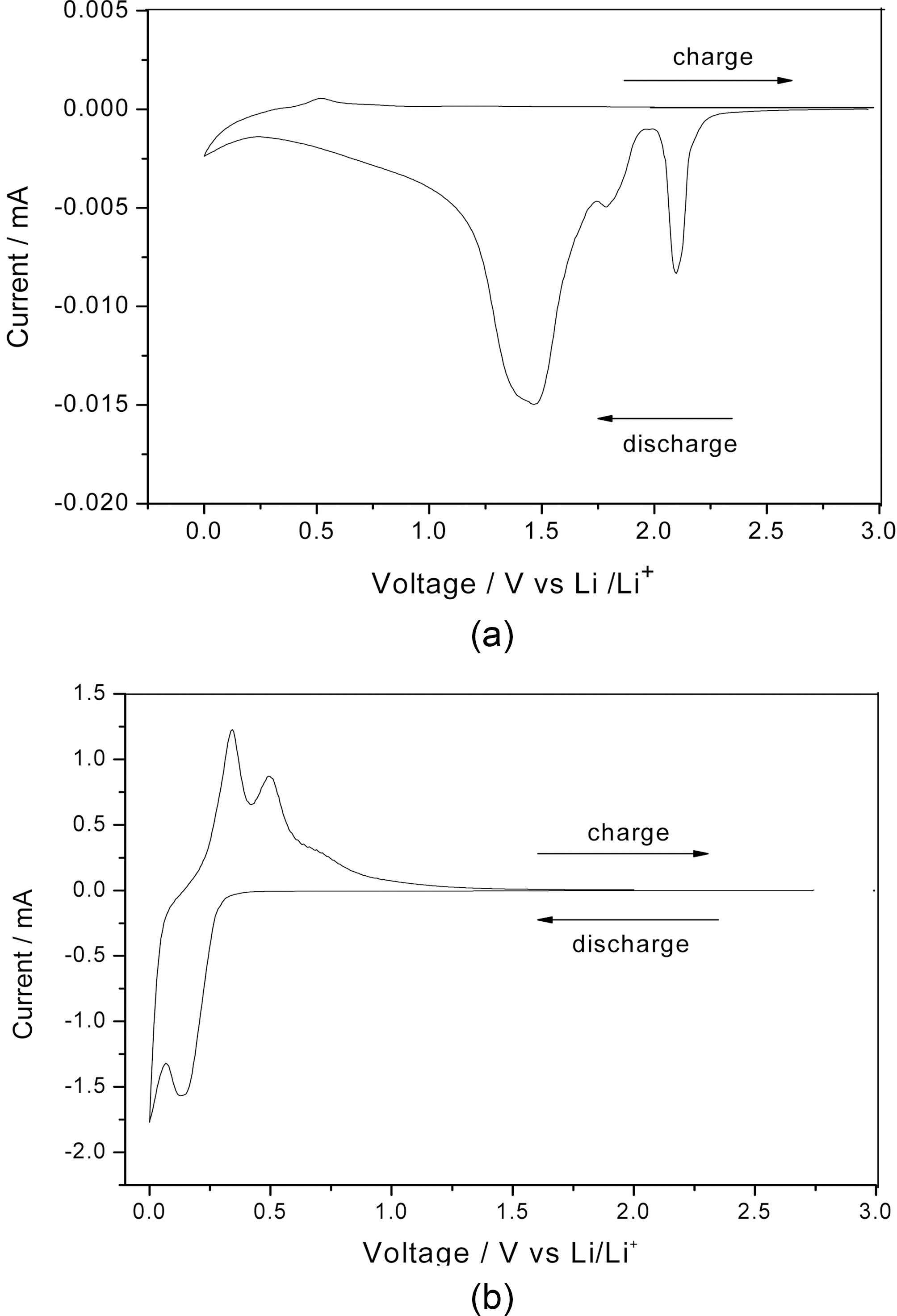
The electrochemical characteristics of the pristine C60 and B:C60 films used as coating layers for silicon films were determined by cyclic voltammetry (CV) measurements. The aim of the CV tests is to investigate the reversible reaction between the lithium ions and silicon film as active materials. The CV curves of the pristine and B:C60 coated silicon films at the first cycle at a scan rate of 0.05 mVs-1 are shown in
Fig. 6. For the pristine C60 coated silicon film, no anodic peaks are detected in the CV profiles. This indicates that the pristine C60 film blocks the insertion of lithium ions into the silicon film used as the active material during the chargedischarge tests. In contrast, the B:C60 coated silicon film exhibits two pairs of cathodic and anodic peaks. It seems that the B:C60 coating layer is effective in preserving the insertion and extraction of lithium ions during the chargedischarge tests. In other words, we can say that the B:C60 coating layer is only acting as an inactive material during the electrochemical tests, the active host material for lithium accommodation is silicon, since the CV profiles of B:C60 coated Si film is similar to that of bare Si film, as reported in our previous paper [15]. Additionally, the current intensity observed in the CV curve of the B:C60 coated Si is higher than that of the pristine C60. Based on the CV results, it can be said that the effectiveness of the argon plasma treatment during the deposition of the B:C60 film in preserving the reversible reaction between the lithium ions and silicon
anode is very significant since it may establish a better path for the transfer of lithium ions at the electrode/electrolyte interface.
In summary, boron doped fullerene (B:C60) thin films were successfully synthesized by a thermal evaporation technique assisted by argon plasma treatment. The presence of boron atoms in the fullerene lattices was confirmed by SEM, XPS and FTIR analysis. The B:C60 film was then utilized as a coating layer for silicon anodes in lithium secondary batteries. The CV results indicated that B:C60 was quite effective in preserving the reversible reaction between the lithium ions and silicon. The argon plasma treatment during the deposition of the B:C60 film contributed to the formation of a passivation layer.