Metal-nitrides have been known to exhibit a number of important properties such as superconductivity, catalytic activity, unusual magnetic properties, and high hardness and mechanical strength [1-7]. Tremendous efforts have been devoted to epitaxially grow binary metal-nitride films such as GaN, TiN, and AlN. Among many synthesizing routes to thin films, metalorganic chemical vapor deposition (MOCVD) and molecular-beam epitaxy (MBE) are the most common techniques for the growth of epitaxial nitride films [8-23]. However, challenges still remain in obtaining high quality epitaxial nitrides. In general, the difficulty in heteroepitaxial growth of high performance nitride films lies in the large mismatches in either lattice parameters or thermal expansion coefficients between the film and the substrate [24,25].
In addition to binary nitrides, great efforts have been made in exploring ternary and complex nitrides since the 1990s [26-36]. However, the materials investigated are mostly in bulk format that were prepared by a standard high temperature "ceramic method". Furthermore, these bulk ternary nitrides very often contain impurities. Thus the intrinsic physical properties of many ternary nitrides have never been well studied. Therefore, single phase epitaxial ternary and complex nitride films are desirable.
The physical vapor deposition (PVD) and chemical vapor deposition (CVD) have the common feature of requiring vacuum systems. An alternative approach for the growth of films is chemical solution deposition, which offers the advantages in terms of the cost, the setup, and the ability to coat large areas [37,38]. The fabrication of thin films by chemical solution approach involves three basic steps: (i) preparation of the chemical solution; (ii) deposition the precursor solution on the substrates by spin-coating, dip-coating, or spray-coating; and (iii) thermal treatments for removing the organic species and crystallization the precursor films to the desired materials under proper environment. Among different chemical solution techniques to thin films, such as sol-gel, metalorganic deposition (MOD), the final two steps are similar. However, the character of the solution chemistry is vital to the quality and properties of the films. In other word, the solubility of the metal precursor, the sensitivity, viscosity and volatility of the solvent, and the reactivity of the mixing of metal precursor and the solvent play important roles in the quality of the final films.
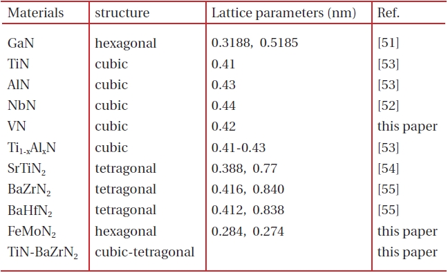
[Table 1.] The nitride films prepared by PAD.

The nitride films prepared by PAD.
There have been some reports on the growth of GaN films by chemical solution deposition [39-48]. These films have been successfully used as buffer layers for the growth of GaN films using MOCVD [39]. However, the precursors used on GaN are not widely available and difficult to handle due to their air-sensitivity. In addition, the morphology of the GaN films needs further improvement as the films were very often non-continuous leading to porous or cracked surfaces. It is apparent that a general versatile chemical solution technique to prepare metal-nitride thin films needs to be developed.
Polymer-assisted deposition (PAD), a novel chemical solution technique, has been developed recently to synthesize high quality epitaxial simple and complex oxide films with desired structural and physical properties [49,50]. In the PAD process, stable metal-polymer solution was used as the film precursor, where the water soluble polymer not only controls the solution viscosity but also binds the metal ions to prevent the metal ions from hydrolysis and to form a homogeneous solution. The solution is air and water insensitive and stable for months and years. Recently, we have extended this technique to prepare epitaxial nitride films. For example, hexagonal GaN [51], superconducting cubic NbN [52], cubic TiN, cubic AlN, mixed Ti1-xAlxN [53], ternary tetragonal SrTiN2 [54] BaZrN2, and BaHfN2 [55] have been successfully prepared by PAD. In this review, we will summarize the nitrides prepared by PAD as shown in Table 1.
In the PAD process, the procedures to form nitride films comprise the formation of a homogeneous metal polymeric liquid precursor, spin-coating the precursor solution on the substrates, and the ammonolysis of the coated films in flowing ammonia gas to yield the metal nitride films. The process begins with the binding of a water soluble metal salt (such as metal nitrate, metal chloride, or metal hydroxide) to a polymer (such as polyethyleneimine [PEI]). Some metal ions bind to PEI directly such as Cu. Some metal ions do not bind to PEI directly such as Ti, but instead bind to functionalized PEI or ethylenediaminetetraacetic acid (EDTA) to form EDTA-metal complex. The major advantage of the EDTA route is that EDTA forms stable complexes with almost all metals. The EDTA complexes further bind to the PEI via a combination of hydrogen bonding and electrostatic attraction. The metal polymeric solution is then purified using Amicon filtration. This removes all material that is of -10,000 g/moL or less, including unwanted anions and cations not binding with polymers. The concentration of the metal in the solution is then determined by inductively coupled plasma-atomic emission spectrometer (ICP-AES).
In detail, Ga-polymer solution, 2 g of gallium chloride was dissolved in 2 g of PEI in 10 g of ethanol. The final Ga concentration is 0.156 M. To prepare Ti-polymer solution, the titanium solution (2.5 g titanium tetrachloride was added slowly to a mixture of 2.5 g of 30% peroxide in 30 mL of water) was added to a solution containing 1 g PEI, 1 g EDTA and 30 mL water until precipitation occurred (the pH was maintained at 7.5). For the Al-polymer solution, aluminum nitrate was mixed with fluorinated PEI polymer (PEIF, prepared by slowly adding 5 mL 48% hydrofluoric acid to 10 g PEI in 40 mL water, while maintaining the pH at 7). Specifically, 2 g aluminum nitrate hydrate was added to 3 g PEIF in 40 mL water. The final concentrations were 0.408 M for Ti and 0.201 M for Al. For Nb-polymer solution, 2 g of NbCl5 were converted to Nb(OH)5 by addition of ammonium hydroxide into the solution. The Nb(OH)5 was then dissolved in 30 mL of deionized water and 7.5 mL of 20% HF. PEI was then added in and mixed. The final solution was 0.4 M Nb. To prepare V solution, 2 g NaVO3 was dissolved in 40 mL H2O followed by adding 2 g PEI. For the Sr solution, 1 g of EDTA and 1 g of PEI were dissolved in 30 mL of water, followed by addition of 1 g of Sr(NO3)2. Using the similar process EDTA-PEI process, metal polymer solutions containing Ba, Zr, Hf, Fe, and Mo were also prepared. The final Sr, Ba, Zr, Hf, Fe, and Mo concentrations were 0.157, 0.216, 0.101, 0.094, 0.209, and 0.376 M.
To prepare binary nitride films, the individual solution is used; to prepare mixed, ternary nitrides or composites, the precursor solution with desired stoichiometric molar ratios is mixed from the individual solutions. The precursor solution was spin-coated on (0001) sapphire (Al2O3) or (001) SrTiO3 (STO) substrates at 2,000 rpm for 30 s. The films were then heated in forming gas (4% H2 and 96% N2) at 510℃ for 2 hours with a ramping rate of 1℃/min and then annealed in ammonia gas at 900-1,000℃ for 2 hours with a ramping rate of 10℃/min. Films with a thickness in the range of 30-40 nm were usually obtained from one spin-coat. It should be noted that film thickness depends on the concentration of the solution by dilution with water and spincoating rate. Thicker films could be always deposited by multiple spin-coats.
X-ray diffraction (XRD) was used to characterize the crystal structure of the films. The surface morphology of the films was analyzed by scanning electron microscopy (SEM) and atomic force microscopy (AFM). The microstructure of the films was analyzed by transmission electron microscopy (TEM). Fourier Transform Infrared (FTIR) absorbance was taken using Nicolet spectrum. The composition of the film was determined by Rutherford backscattering spectrometry (RBS). The optical properties of the films were examined by ultraviolet-visible (UV-Vis) transmittance at room temperature. The electrical resistivity (Ω) was measured from 5-300 K using a standard four-probe technique by a Quantum Design Physical Properties Measurement System (PPMS).
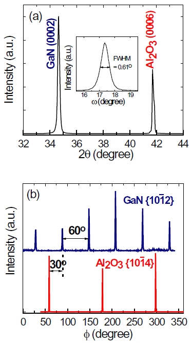
Figure 1 shows the XRD θ -2θ scan, rocking curve, and φ -scans of a GaN film on sapphire substrate annealed in ammonia gas at 900℃ [51]. Only (0002) peak from hexagonal GaN is observed, indicating that the film is preferentially oriented along the
3.2 Cubic TiN, NbN, VN, metastable AlN, and mixture Ti1-xAlxN on SrTiO3
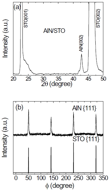
The XRD patterns for TiN, AlN and mixed Ti1-xAlxN films on SrTiO3 (STO) substrates are similar since the lattice parameters of cubic TiN and AlN are very close (
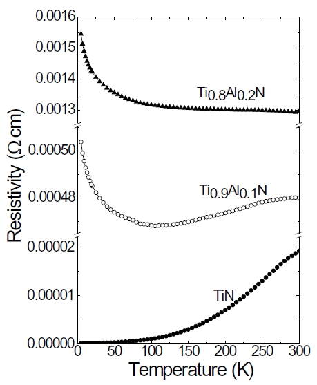
As expected, AlN film is insulator but has an optical transmittance greater than 75% at wavelengths in the range of 300-1,100 nm. TiN film is highly conductive with a room temperature resistivity of around 1.9 × 10⁻⁵ Ω.cm. The room-temperature resistivity increases with increasing Al content while the transmittance decreases with increasing Ti content in Ti1-xAlxN films. Figure 4 shows the temperature dependence resistivities of TiN film annealed at 900℃ and Ti1-xAlxN (x = 0.1 and 0.2) annealed at 1,000℃. The resistivity decreases as the decrease of temperature. On the other hand, the Ti0.9Al0.1N film is metallic between 300 K and 100 K and changes to semiconductor behavior from 100 K to 5 K. With further increasing Al content in Ti1-xAlxN (x = 0.2 - 0.5) films, a semiconductor behavior is shown from 300 K to 5 K.
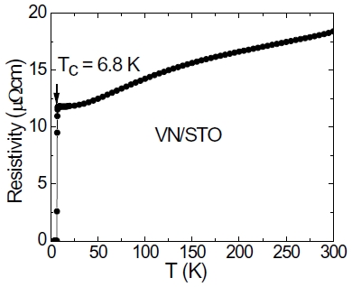
The cubic NbN and VN prepared by PAD have the similar XRD patterns as TiN and AlN. High quality epitaxial superconducting NbN films with a transition temperature Tc of 14 K have been obtained although the lattice mismatch between NbN and STO is 12% [52], indicating that PAD route provides an alternative approach for the preparation of epitaxial films on substrates with large lattice mismatch. We also succeeded to get superconducting epitaxial VN films on STO. Figure 5 shows the plot of resistivity vs. temperature. The resistivity increases with the temperature from 7 K to 300 K, indicating a metallic behavior. A superconducting transition at temperature of 6.8 K is clearly seen for VN films.
3.3 Tetragonal SrTiN2, BaZrN2, BaHfN2 on SrTiO3
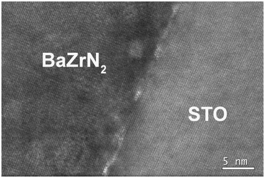
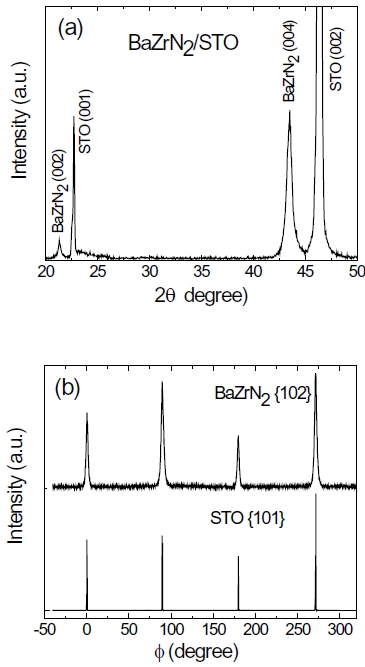
SrTiN2, BaZrN2, and BaHfN2 crystallize in the layered KCoO2 structure with a space group P4/nmm, where Ba2+ sits between layers of edge-sharing [ZrN2]2- or [HfN2]2- square pyramidal anions. The relatively small in-plane lattice mismatch between these metal-nitrides and STO makes it possible to epitaxially grow these materials in film form. Figure 6 shows the XRD results from the θ -2θ scan and φ -scan of BaZrN2 film on STO substrate annealed at 1,000℃ for 1 hour [55]. The appearance of (002) and (004) peaks from tetragonal film together with (001) and (002) peaks from the substrate indicate that the films are preferentially oriented along the c-axis perpendicular to the substrate surface. It should be noted that no other detectable second phase material was observed, in contrast with ceramic ternary metalnitrides where binary nitrides are often observed. The in-plane orientation between the films and the substrates was determined by XRD φ -scans from the (102) peak of BaZrN2 and (101) peak of STO, respectively. The epitaxial relationships between these films and the substrate can be generally described as (001)film''(001)STO and [102]film''[101]STO. These tetragonal ternary nitride films are very dense, smooth and uniform. Figure 7 shows the HRTEM image on BaZrN2 film on STO. The interface is flat and clean.
Our ability to fabricate single phase epitaxial ternary nitride films allowed us to investigate their physical properties. SrTiN2 is a transparent semiconductor with a direct band gap of 3.65 eV [54]. BaZrN2 and BaHfN2 films are highly metallic but no superconducting transition temperature is observed [55].
3.4 Hexagonal FeMoN2 on sapphire
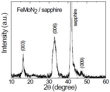
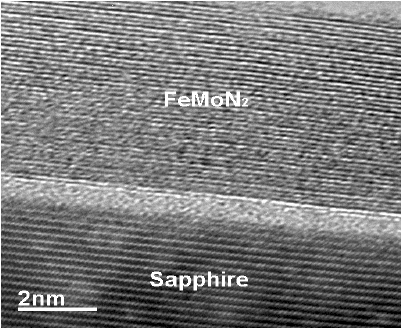
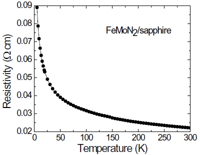
FeMoN2 crystallizes a hexagonal WC structure with lattice parameters of a = 0.284 and c = 0.274 nm. Figure 8 shows the XRD pattern of the FeMoN2 film on sapphire annealed at 1,000℃. The θ -2θ scan shows the (003), (006), and (009) peaks from the film, which indicates the film is preferentially oriented along the c-axis perpendicular to the substrate surface. However, the in-plane orientation of the film to substrate is not observed. Figure 9 shows the cross-section HRTEM image. It is clearly seen that the film is hexagonal and epitaxial grown on sapphire. However, the film is very thin with thickness of around 5 nm. If we increase the film thickness, the film contains binary MoN from XRD analysis, no longer a single phase of ternary nitride. Figure 10 shows the resistivity as a function of temperature curve, FeMoN2 exhibits semiconductor behavior, different from the metallic behavior reported for FeMoN2 powder [36]. Scattering from grain boundaries and carbon or oxygen contamination at the grain boundaries in the films can all contribute to such effect.
It is noted that for mixed nitrides or ternary nitrides, the metal ratio and carbon and oxygen contamination have been measured with resonant RBS. The nitrides films do contain some carbon and oxygen, however, the data analysis for carbon and oxygen based on RBS are quite hard without reliable standards.
3.5 Nitride nanocomposite TiN-BaZrN2 on SrTiO3
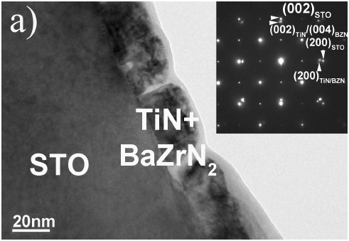
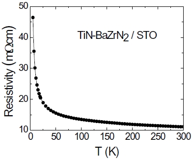
The PAD technique demonstrates a promising approach to synthesize single-phase ternary nitride thin films by simply mixing different metal polymer solutions. We also find that PAD can be used to prepare even complex nitride system. Here we use TiN-BaZrN2 nanocomposite as an example. To the best of our knowledge, there is no report on self-assembled nitride nanocomposite films. The precursor solution for the growth of TiNBaZrN2 nanocomposite films (molar ratio is 1:1) was prepared by mixing individual aqueous solutions of Ti, Ba, and Zr with polymers. Self-assembled epitaxial nanocomposite films were accomplished by annealing the precursor films in flowing ammonia at 1,000℃ for 1 hour. The XRD results show that the TiN (002) peak is close to the BaZrN2 (004) peak. It is expected that the epitaxial relationships of the composite on substrate can be described as (002)TiN''(004)BZN''(002)STO and [101]TiN''[102]BZN''[101]STO. Figure 11 shows cross-section HRTEM image of a TiN-BaZrN2 film on STO substrate. The composite grows like island structure and TiN phase seems to be at the gap of BaZrN2 phase and top surface. The cross-section HRTEM image and SAED pattern taken from the interface show the epitaxial relationships between the two phases and the substrate. The reason of TiN mostly on the top surface of composites is probably due to the lower density of TiN compared with BaZrN2. It is interesting to note that the composite shows semiconductor behavior, as shown in Fig. 12, while both single phase TiN and BaZrN2 are highly conductive [53,55]. Again the grain boundary between the two phases can dominate the resistivity vs temperature behavior of the films.
In conclusion, the successful growth of epitaxial hexagonal GaN, cubic TiN, AlN, NbN, VN, mixed cubic Ti1-xAlxN films, ternary nitride tetragonal SrTiN2, BaZrN2, BaHfN2, hexagonal FeMoN2, and self-assembled nanocomposites TiN-BaZrN2 films with desired structural properties indicates that PAD is an alternative approach for epitaxial nitride films. The polymer used to form the stable and homogeneous precursor solution plays an important role to form these materials.

![X-ray diffraction patterns: (a) θ -2θ scan of GaN film on sapphire. Inset shows the rocking curve of (0002) reflection; (b) φ -scans from (10 12) reflection of GaN and (10 14) reflection of sapphire (Ref. [51]).](http://oak.go.kr/repository/journal/10145/E1TEAO_2010_v11n2_54_f001.jpg)

![X-ray diffraction patterns: (a) θ -2θ scan for AlN/STO; (b) φ-scans from (111) reflections of AlN and STO (Ref. [53]).](http://oak.go.kr/repository/journal/10145/E1TEAO_2010_v11n2_54_f003.jpg)
![Temperature dependent resistivity of a TiN film annealed at 900℃ and Ti1-xAlxN (x = 0.1 and 0.2) films on STO annealed at 1,000℃ (Ref. [53]).](http://oak.go.kr/repository/journal/10145/E1TEAO_2010_v11n2_54_f004.jpg)
![X-ray diffraction patterns: (a) θ -2θ scan and (b) φ -scans from (102) reflections of BaZrN2 and (101) of STO (Ref. [55]).](http://oak.go.kr/repository/journal/10145/E1TEAO_2010_v11n2_54_f006.jpg)