Tin oxide has been widely studied as a transparent conducting oxide, with applications, for example in optoelectronics, photovoltaics, as a catalyst, and as a gas sensor. SnO2 films have been fabricated using many different technologies, including sputtering [1], chemical vapor deposition [2], spray pyrolysis [3], and atomic layer deposition (ALD) [4], [5]. Amongst these ALD produces unique film properties compared with other methods. In particular dense films of high aspect ratio and fewer defects are achieved. ALD is also an ideal technology for the deposition of ultrathin films with high conformality and precise thickness control [6]. ALD is a dense thin film growth technology using an alternating self-controlled chemical process between the gas precursor and a solid surface in order to deposit materials in an atomic layer-bylayer fashion. This methodology can produce films with very precise control over film thickness and composition. This technology allows precise coatings to be applied on other surfaces of powder and porous materials. Plasmaenhanced ALD (PEALD) is a promising technology for obtaining high quality metal oxide films at relatively low temperatures compared with commercial CVD. Interestingly, the comparative study of the growth of tin oxide films by ALD and chemical vapor deposition was reported [7]. The films were of the tetragonal rutile-type for both cases. Thin films grown by ALD were found to be close to being perfect single crystals, containing a low density of defects and were almost atomically smooth. The CVD films had a much rougher film morphology and exhibited both grain boundaries and twin formation.
Tin oxide thin films have been fabricated previously by ALD using halogenated precursors, SnCl4 and SnI4, and non-halogenated precursors, tetrakis (dimethylamino)tin and dibutyltin diacetate [4], [5], [8]. By using halogenated precursors, high deposition temperatures and low growth rates with corrosion problems were reported. Amongst nonhalogenated precursors, dibutyltin diacetate produced tin films with an 8 sec purging time at 50 ∼ 300℃ [4]. They investigated the annealing effect of tin oxide film and XPS analyses with various deposition temperatures. The dominant oxygen species for 100-, 200-, and 400- growth cycles in the as-deposited films are O2 -, O-, and O2-, respectively.
From the non-halogenated precursor tetrakis (dimethylamino)tin, tin oxide film was deposited at an average growth rate of 1.2 A/cycle at 50 ∼300℃ by using a seeding method for the ALD [5].
In this research, we prepared thin oxide film by plasmaenhanced ALD by using tetrakis (ethylmethylamino) tin as a new non-halogenated precursor, with different temperature ranges. The analyses of the thin films, as-deposited and thermally annealed, were performed.
The ALD experiment used a bubbler type source delivery system with separately installed gas purge lines. Tin oxide was grown as an insulating layer on a 4” p-type Si (100) wafer after plasma cleansing. The tin oxide precursor was tetrakis(ethylmethylamino) tin. Oxygen plasma was used as an oxygen source. The reaction temperature of the process module was controlled in the temperature range of 50℃ and 200℃. The reactor pressure was maintained at 0.8 Torr with an Ar purging of 100 sccm. During the reaction tetrakis (ethylmethylamino) tin and oxygen plasma were sequentially injected into the reactor chamber to form a tin oxide monolayer on the substrate. The ALD cycle consisted of the injection of tetrakis(ethylmethylamino) tin for 4.0 s, Ar for 20 sec, O2 gas for 2 sec, and additional 2 sec with an radio frequency (r.f.) power of 100 W, and a final gas purge for 20 sec. The crystalline phase of the tin oxide film was characterized by X-ray diffraction (XRD, Philips, Holland) using Cu-Ka radiation operated at 35 KV. The microstructure was examined by the use of a field emission scanning microscope (FE-SEM, Joel, Japan). The surface morphology was examined by AFM (PSIA, XE-150, Korea) and an ellipsometer (Gartner L116D, US) was used for thickness analysis. XPS analysis was performed by means of a Thermo VG ESCA Sigma Probe spectrometer (U.K.) using a monochromatric Al-Ka radiation source from an X-ray source operated at 15 kV and 100 W. The surfaces of the specimens were cleaned by Ar+ etching (2 kV, 1.8 μA) prior to recording a spectrum. The spectra were calibrated by C 1s (285 eV).
Tin oxide was prepared by ALD with a non-halogenated precursor. Non-halogenated precursors have some advantage over halogenated ones. Tetrakis(ethylmethylamino) tin i.e. [Sn(N(CH2CH3)(CH3))4], is a new non-halogenated precursor that was prepared specifically for this research. This precursor is a moisture sensitive yellow liquid. It is soluble in hydrocarbons with the molecular weight of 351.12 g/mol, and a boiling point of 100℃/0.4 torr (301℃/760 torr). Initially, the process conditions and control parameters were tested to ensure thin film formation. From previous results, reactants as oxygen sources, such as water, H2O2, oxygen plasma and O3 were used. Amongst these, H2O2 showed the highest growth rate.
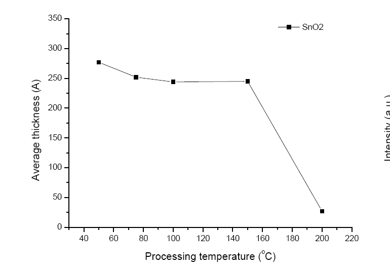
Figure 1 shows the average growth rate of tin oxide thin film as a function of substrate temperature. At low temperatures, the average growth is over 1.2 A/cycle. However, the growth rate dramatically decreases to almost no film formation at 200℃. There was no chance of the nucleation of tin oxide at temperatures higher than this. Generally, the growth rate of tin oxide by vacuum deposition methods such as ALD, CVD, and sputtering is relatively high at low temperatures and decreases with the increasing temperature. Previous results obtained with other precursors and hydroxyl peroxide reactant reported that the average growth rate of tin oxide by ALD was 1.2 A/cycle between 100℃ and 200℃, and the rate dropped above 250℃ [5]. Our results shows very similar growth rates but with the rate falling rapidly at a lower temperature of 200℃. The previous workers used a seed material consisting of a 1 nm thickness of Al2O3 with trimethyl aluminum. Without seeding of initial Al2O3 step, thinner SnO2 film showed greater thickness variation [5].
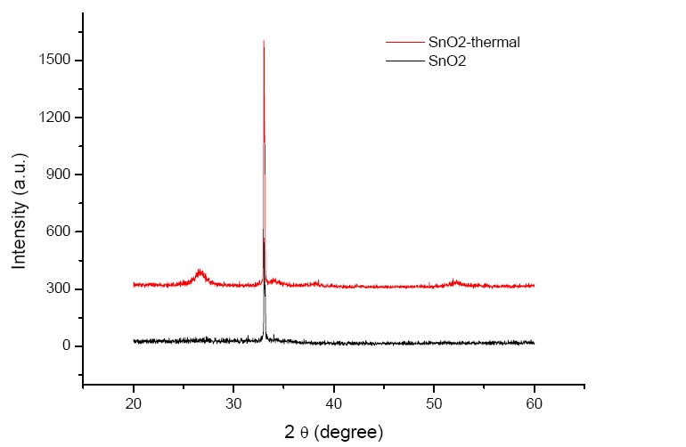
From the XRD characterization in Fig. 2, the crystallinity of as-deposited film is not observed at the substrate temperature of 150℃. However, a (110) peak appears as dominant after being thermally annealed at 600℃ for 30 min. Interestingly, the trace of the (220) peak around 53 degrees, the (101) peak around 34 degrees, and the (200) peak around 39 degrees are detected after thermal annealing. The (110) crystalline surface of the tin oxide is thermodynamically the most stable and the predominant crystal face [9].
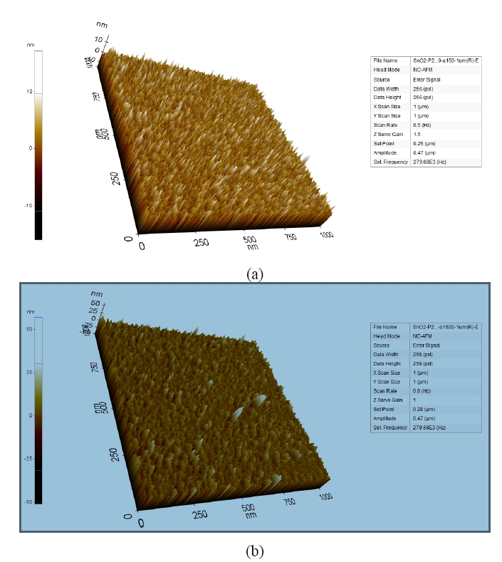
The surface morphology of the two tin oxide samples, asdeposited and thermal annealed, were characterized by AFM. Dense tin film produced by ALD was observed as expected. The Rq (root mean square roughness) and Ra (average roughness) of the as-deposited tin film are 2.64 nm and 2.09 nm respectively, whilst the Rq and Ra of the thermally annealed films are 5.88 nm and 4.64 nm, respectively. An especially interesting feature is that the roughness is relatively good, even though the grain levels are increased after thermal annealing. Post-annealing results show a more pronounced texture and grain growth. The morphology and roughness variation of thin films, in general, are due to the coalescence or migration of grains.
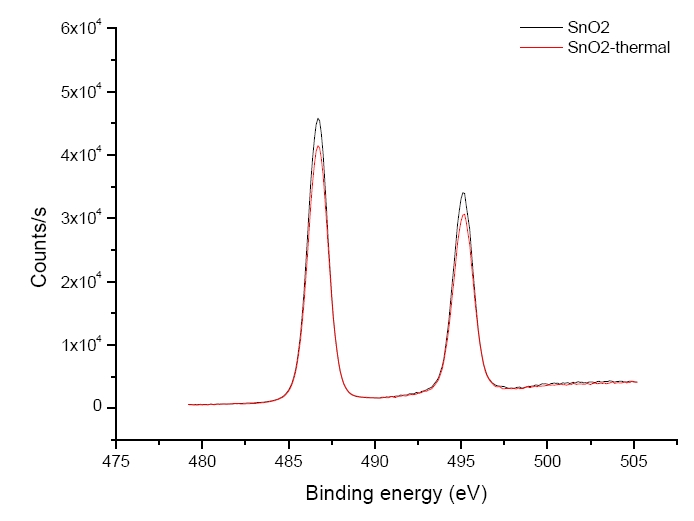
XPS measurements were performed to verify the dependence of the tin oxide components and composition on process conditions and thermal treatment. Figure 4 shows the XPS data of the Sn 3d spectra of the 200 cycle films asdeposited at 50℃ and the thermally annealed film. The binding energies of the Sn4+ peak and Sn2+ peak are 487.2 eV and 486.25 eV, respectively. The binding energies of the Sn4+ and Sn2+ peaks were assigned 486.5 and 486.25 eV in the literature [10], However, the assignment depends on the process parameters. Because the analytical resolution of the XPS technique within 0.01 eV is limited by the instrument, separation of the Sn4+ and Sn2+ peaks is difficult. The binding energy of the Sn 3d5/2 peak can be assigned as 486 eV.
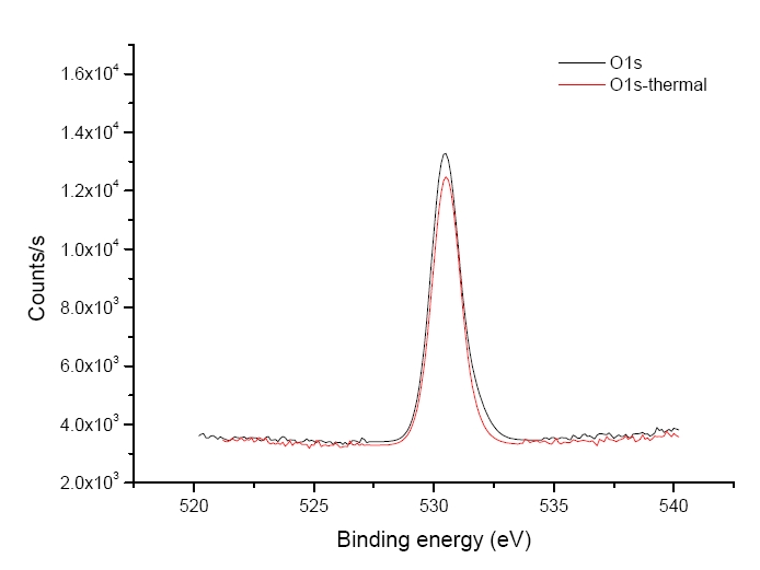
The XPS measurement of oxygen in a tin oxide film shows in Fig. 5. Different types of oxygen status can demonstrate various binding energies, such as 530.70 eV for O-, 530.15 eV for O2-, and 530.6 eV and 532.8 eV for O2 -. These oxygen statuses also are affected by the process parameters. From Fig. 5 the single peak of 530 eV might be assigned to either O- or O2-. The atomic ratios of [Sn] : [O] in the XPS spectrum are estimated to be 45.72 : 54.28 for the as-deposited and 46.80 : 53.20 for the thermal annealed films, respectively. The tin amount in the tin oxide composition increases slightly with thermal annealing. XPS spectra show no contamination by carbon in the tin oxide films.
In order to prepare tin oxide thin films by ALD, a new precursor tetrakis(ethylmethylamino) tin was prepared. The average growth rate of the tin oxide film is about 1.2 A/cycle in the temperature range from 50℃ to 150℃. The growth rate decreases rapidly at a substrate temperature of 200℃. ALD-grown tin oxide thin film was characterized using XRD, AFM and XPS. The roughness of the deposited tin film was good. The atomic ratios of [Sn] : [O] in the XPS spectrum are estimated to be 45.72 : 54.28 for the asdeposited and 46.80 : 53.20 for the thermal annealed films, respectively. The surface roughness, tin amount in the composition and crystallinity increased with thermal annealing.