Conventional lithography using a mask was invented in the 18th century. Even now, most of the lithography carried out uses masks. Due to the problems caused by masks such as expense and time in fabricating the masks, contamination by masks, disposal of masks, and the alignment of masks, research on maskless lithography was initiated. Recently, Spatial Light Modulator (SLM) devices for Micro Electro Mechanical System-based (MEMS-based) digital light processing have brought innovation to the microdisplay field. These SLM devices include the Digital Micromirror Device (DMD) by Texas Instruments Inc. and some other SLMs) [1-5]. Nowadays, many new application fields for them have emerged. One of them is maskless lithography for semiconductor and Flat Panel Display (FPD) fabrication [3-10].
In the maskless lithography described in this paper, the micromirror array works like a mask to write patterns directly onto substrates. In comparison with other maskless lithography technologies, the micromirror based lithography technology possesses superior features. It is characterized by sufficient throughput for highly customized patterns, fine lithographic quality, efficiency in cost and time [9], and so on. Nevertheless, the micromirror based lithography is feasible if, and only if, each system developer could set up an excellent optic unit [10, 11], and an accurate DMD control unit [3-8, 12]. To fabricate lithographic patterns, millions of micromirrors on the DMD need to be addressed and adjusted, individually and instantaneously. However, detailed discussion on the DMD control is beyond the scope of this paper. The details on the DMD control associated with the proposed system can be found in the literature [8, 12].
Due to increasing demands for small electronics, the Printed Circuit Board (PCB) circuit pattern size has been decreased gradually and is now down to 10 μm. Therefore, the optical system [12] developed for Plasma Display Panel (PDP) fabrication which has 30 μm resolution can not be used for PCB fabrication. A new optical system is needed. This study is focused on the development of a 4 μm resolution optical system for high resolution maskless lithography using the DMD for PCB fabrication.
II. DESIGN OF OPTICAL SYSTEM FOR MASKLESS LITHOGRAPHY
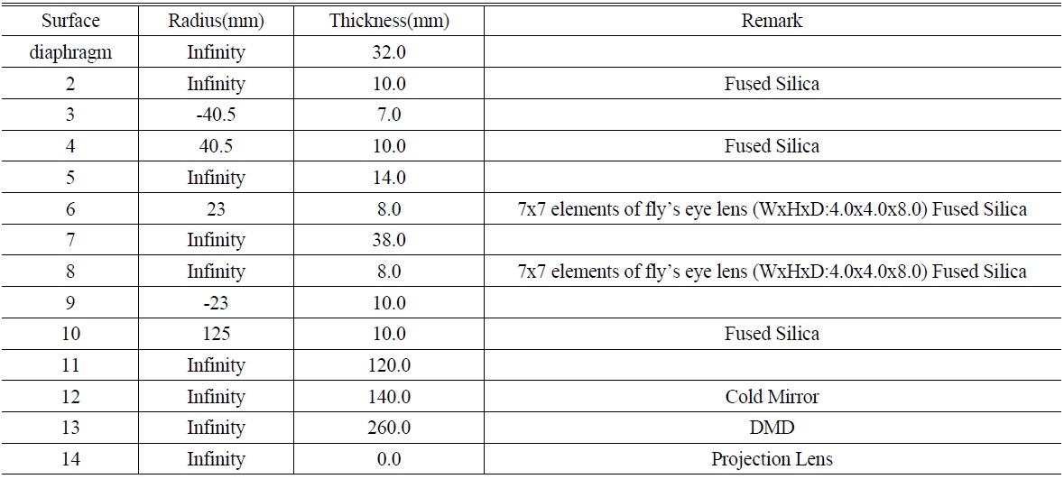
The proposed system consists of an illumination optical system, a DMD, and a projection lens system. The illumination optical system composed of fly's eye lens plates, a 405 nm NBPF, condensing lenses, a field lens and a 250W halogen lamp is developed to achieve 95% uniformity. The projection lens system, composed of 8 optical elements, is developed for 4 μm resolution.
2.1. Design of illumination optical system
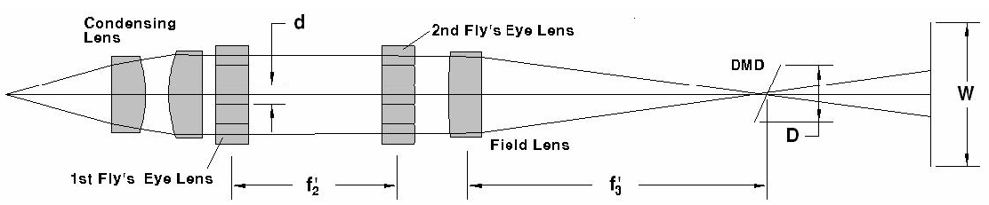
Success of the design for an illumination optical system depends on two design strategies; one is to achieve the high uniformity of the illumination beams on the DMD surface and the other is to achieve the complete incidence of all the illumination beams reflected from the DMD surface upon the effective aperture of the projection lens. For uniform illumination on the DMD surface, we designed a beam homogenizer using fly's eye lens plates, and for the illumination beams to be incident upon the effective aperture of projection lens, we properly adjusted the distance between the first and second fly's eye lens plate, the curvature radius of the unit cell of the fly's eye lens, and the focal length of the subsequently arranged field lens.
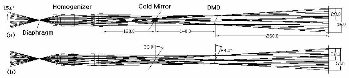
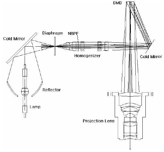
In the design, we used a 250W halogen lamp supplied by USHIO Co. and we used a NBPF to utilize the line width of 405nm ±2 nm. As to the reflector of the lamp, we used only the 47.4 mm depth section ranging from one end of the major axis of an ellipsoid with major axis of 252 mm and minor axis of 128 mm. The inner surface of the reflector was coated to be a cold coating mirror at 350~480 nm wavelength. As a result, according to the simulation, the illumination beams reflected from the lamp were collected on the focus with about ±15° angle of convergence. Then we let the collected illumination beams pass through a variable diaphragm which acts as a pinhole with a 3~5 mm diameter. To make these illumination beams uniformly illuminate the DMD surface and to let all of them again enter into the effective aperture of projection lens, we let all of them pass through a beam homogenizer consisted of condensing lenses, two fly's eye lens plates, and a field lens. A configuration of the initial design of the homogenizer is given in Fig. 1.

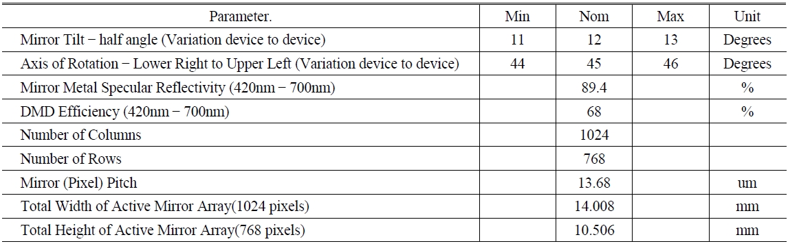
Optical and physical parameters of DMD(quoted from DMD 0.7 XGA LVDS DMD Discovery™ Product Preview)
If the cell width of the fly's eye lens is
Where,
As specified in Table 1, the tilting angle of the micro-vertically against the horizontally positioned homogenizer only when the DMD surface is tilted against the optical axis of the illumination beams at an angle of 66°. Given that the effective diagonal size of DMD is 17.51 mm (calculated from the parameters of DMD in Table 1), the optimum area needed for homogenous illumination is the elliptical shape with long axis of 17.51 mm and short axis of 16 mm(=17.51×cos24°). Considering factors such as assembling tolerance of the homogenizer, there is a need to extend the uniform illumination area to about 18 mm in the initial design. Therefore, if we let D be 18.00 mm,
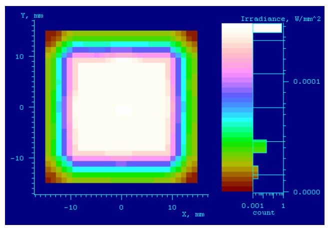
Based on these, Table 2 and Fig. 2 show the optimized design data and configurations taking into account the actual thickness of lenses. As depicted in Fig. 2, the illumination beams starting from the lamp pass through a 3 mm diaphragm and fly's eye lens plates almost in parallel by means of two condenser lenses. Fig. 2(a) shows ray tracings of the illumination beams that radiate from the center of the diaphragm at an angle of ±15°. It shows the illumination beams going through a cross section made up of a 49-element fly's eye lens plate, of which the cell dimension is 4 mm in height, 4 mm in width, and 8 mm in depth, passing through the homogenizer and the effective size of the DMD, and entering into the effective diameter of the projection lens. Fig. 2(b) shows that the illumination beams, which radiate from the edge of the 3 mm diaphragm, pass through the homogenizer and the effective size of the DMD, and are able to enter into the effective diameter of the projection lens. If the illumination beams fail to pass through the real DMD size, they won't be reflected by the micromirror of the DMD and thus cannot be incident upon the projection lens. Hence, in Fig. 2(a) and (b), the rays of illumination beams not passing through the real DMD size (14.008 mm × 10.506 mm from Table 1.) can't be reflected toward the projection lens and, therefore, do not need to be taken into account when calculating an effective aperture of the projection lens. Finally, by real ray tracings, we could confirm that the illumination beams, which are to pass through the real DMD size and be incident upon the projection lens, are within 52 mm of the projection lens in diameter, which implies that the effective diameter of the projection lens should be 52 mm or more. Also, this implies that the initial paraxial marginal ray angle should be (수식처리)and the object numerical aperture (NA) is 0.1, which should be used in the next section. Fig. 3 shows the simulation results of the illumination beam distribution by the designed illumination optical system at the position of the DMD. We conclude that 95% or more uniformity can be achieved in the area of 18 mm×18 mm.
[TABLE 2.] Data of the optimized homogenizer
Data of the optimized homogenizer
2.2. Design of projection lens system
Among the objective lenses for projection, the Biotar (DoubleGauss) type is used widely because the optical properties of meniscus lenses which are presented symmetrically inside the system are superior to lenses of other types. Thus, many high-performance lenses are designed by adopting a variant of this type. Also, we would like to find the numerical solutions of the initial design by adopting the Biotar (DoubleGauss) type [13]. However, in the DMD projection optics, because the NBPF passes only the light of a narrow band of 450 nm±2 nm wavelength, chromatic aberrations are not important. In the process of determining the initial solution, therefore, we did not need to consider the chromatic aberrations and use only unique index of refraction in order to determine the initial solution promptly. (Actually, we use only FD8 as lens material.)
Finally, in using the Biotar type design, we could isolate the cemented lenses in order to have more degrees of freedom which provide more favorable conditions to find the initial solutions.
Thus, the initial design conditions appropriate to our maskless optical system could be set down as follows:
1) The DMD composed of 1024×768 pixel in which the unit cell size is 13.68 μm×13.68 μm has the overall size of 14.008 mm×10.506 mm. So, in order to make a unit cell image of 4.0 μm×4.0 μm in the substrate, the magnification(mβ) should be -0.2924x.
2) All five kinds of the third-order aberrations should be zero.
3) The telecentricity in image space should be zero.
4) Considering the placement and the space of the homogenizer and the illumination reflection mirror of the DMD optical system which let the illumination beams go toward the DMD, the distance from the DMD plane to the first surface of the projection lens should be 260 mm.
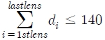
5) The distance from the first surface to the last surface of the projection lens should be less than 140 mm.
6) The working distance from the substrate should be at least 30 mm.
In order to create a computer program to obtain initial solutions, we can summarize the above initial designing conditions as follows using the analytical formulas.


(For 6 elements,
Where,
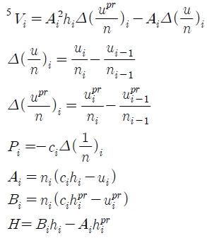
In these equations,
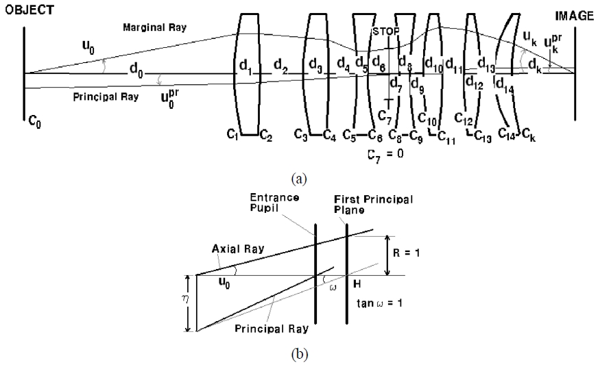
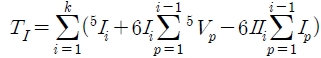
The schematic diagram of the DMD projection system is shown in Fig. 4(a). We want the solutions which are free from all third-order aberrations (
But the value of the fifth-order spherical aberration (Eq. 12) is only used to compare the initial solutions. In other words, by comparing the value of the fifth-order spherical aberration and by selecting the solution with a smaller value, we can choose the solution with a good condition for optimization.
The above fifth-order spherical aberration is Matsui's expression. Because Matsui's expression [16, 17] is more compact than Buchdahl's [18], we prefer to use his expression. Then, in using Matsui's expression, we should give any restrictions to
Therefore, the desired initial solutions of the DMD projection system should satisfy the Eqs. (2)~(9) and the restrictions of (10) and (11).
Therefore, the desired initial solutions of the DMD projection system should satisfy the Eqs. (2)~(9) and the restrictions of (10) and (11).
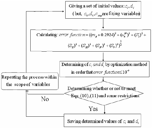
The program producing the initial solutions uses the optimization method which uses the damping least square method [19], and its algorithm is shown in Fig. 5.
For an 8 element projection lens, by properly applying initial values of 35 variables (really,

becomes 10-9 or below. To prevent the solution from being a local minimum, initial solutions were repeatedly obtained by allowing 33 variables to be selected variously within the potentially feasible specific areas. Similarly, initial solutions were calculated for 7 or 6 element projection lenses.
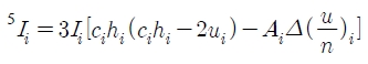
The fifth spherical aberration (δ
In this equation, R is the height of the paraxial marginal ray in the entrance pupil.
Eqs. (14) is used for calculating the residual fifth spherical aberration of each initial solution. Here,
[TABLE 3.] Optical characteristics of the initial numerical solutions

Optical characteristics of the initial numerical solutions
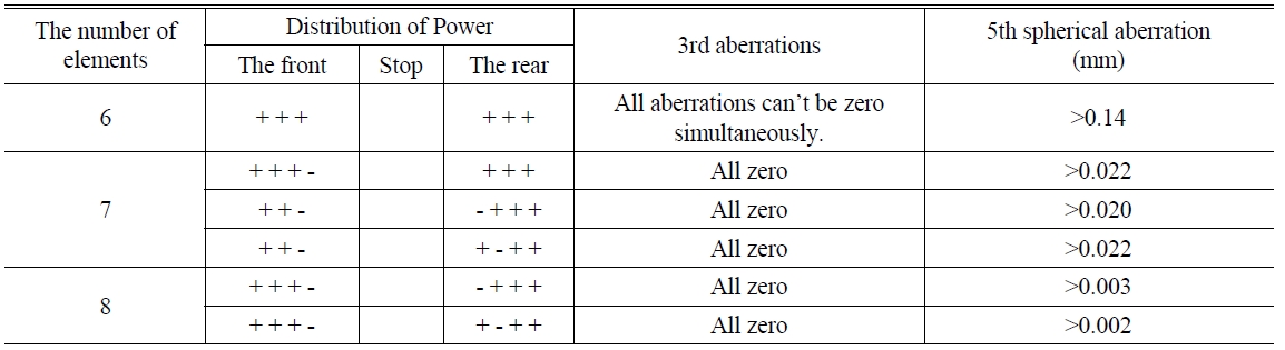
For the 6 element system, not all of the third-order aberrations can be eliminated and thus this system is not suitable for our purpose.
For the 7 element system, the initial solutions were obtained either when a lens was added to the front of the stop or the back of the stop. As a result, it was confirmed that the third-order aberration was all eliminated for the initial solution and the amount of the residual fifth-order spherical aberration was 0.02 mm or more. In case of the 7 element system mentioned above, It had the residual spherical aberration larger than 20 μm, so it was considered to be a low-profile system that could not give the resolution of below 4 μm, and it was true when we optimized it.
The 8 element system is a system that added two lenses on the front/back in a separated Biotar(DoubleGauss type) lens system, and the distribution of its refraction power is +,+,+,-, (stop), +,-,+,+/ +,+,+,-, (stop), -,+,+,+ and the thirdorder aberrations are all eliminated and the amount of the residual fifth-order spherical aberration is 0.002 mm or more. Among those initial solutions gained, we selected a proper initial solution for optimization with a consideration of feasibility of fabrication, related data and configurations are given in Table 4 and Fig. 6.
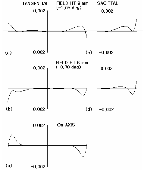
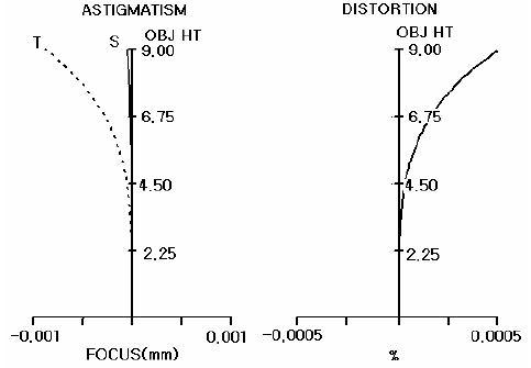
Fig. 7 shows the residual finite ray aberrations of the selected initial solution of which the object numerical aperture (NA) is (수식삽입)and proves that at least 2 or more high-order aberrations are left in the on-axis aberration diagram (Fig. 7(a)) presented the spherical aberration. Because at present the total residual spherical aberration is about 2 μm or less, it is confirmed that there is no need to gain initial numerical solutions by adding lens to further remove high-order spherical aberrations. That is, it is possible to further reduce the marginal aberration value of the residual spherical aberration in the optimization process by combination of the third, fifth, and seventh order spherical aberration, so it is rational to conclude that there is no need to gain numerical solutions by adding more lenses to simultaneously remove the third and fifth order spherical aberration. Fig. 8 shows the astigmatism and distortion of the selected initial solution and proves that the astigmatism and distortion is almost absent for the full field.
[TABLE 4.] Design data of the selected initial projection lens solution
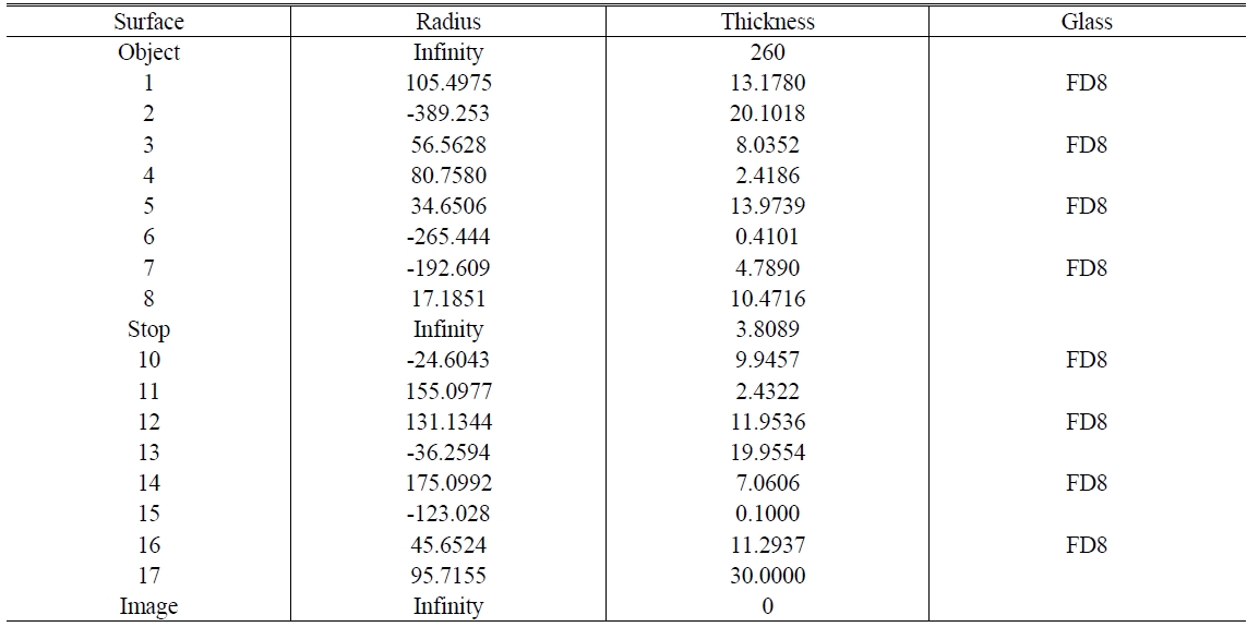
Design data of the selected initial projection lens solution
2.3. Optimized design of projection lens system
We induced and selected an initial solution for the 8 element system in the previous section, and now we have to optimize it to make it consistent with our system.
First of all, we did not consider chromatic aberrations at all while obtaining the initial solution. Therefore, it is necessary to gain the optimized solution with lens material as a variable in the optimization process. In addition, we should perform the optimization process by considering the depth of focus of ±1.73 μm on the image surface which is related with the moving precision of the base plate of the user stage and the objective numerical aperture of 0.1.
[TABLE 5.] Design data of the optimized projection lens
Design data of the optimized projection lens
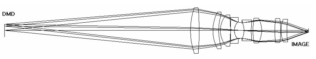
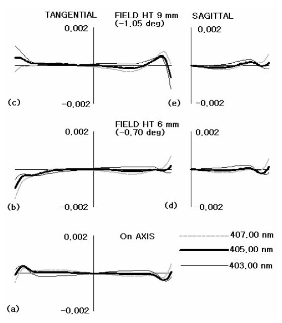
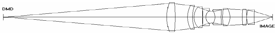
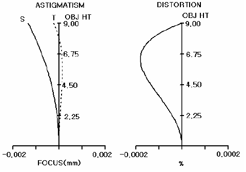
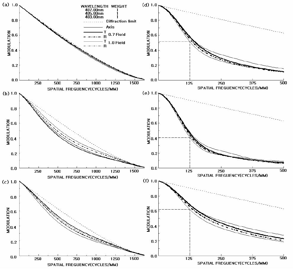
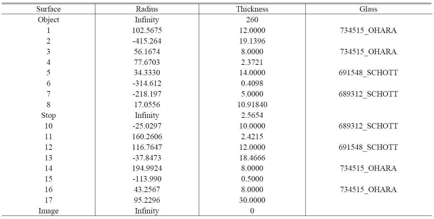
Table 5 and Fig. 9 show data and configuration of the projection system optimized by the above process. Fig. 9 shows the -0.292× projection system that is able to project mask patterns which are generated by the micromirror of the DMD and exposed on the base plate when the uniform illumination beams are irradiated on the DMD surface and reflected on the micromirror of the DMD. This optical system is designed to maintain the image telecentricity so that to accommodate tiny errors along the optical axis on the base plate of the stage. Since the size of micromirror of DMD is 13.68 μm×13.68 μm, the formed image becomes 4 μm×4 μm. Fig. 10 shows the residual finite ray aberrations of the optimized projection lens and proves that 2 μm or less residual aberrations are left in all of the fields. In particular, Fig. 10(a) shows the residual spherical aberration is 0.5 μm or less. Fig. 11 shows astigmatic and distortion aberrations, indicating that there is almost no distortion within 5.26 mm(mβ'×18 mm) of a diameter of image field on the substrate. Fig. 12 shows various MTF curves of the optical system. At Fig. 12 (a), (b), (c), we know that the line width of resolution is about 1.14 μm for the depth of focus of ±1.73 μm based on the 50% modulation criterion. In reality, however, the line width would be about 4 μm, taking into account the fabrication tolerances of the lenses and barrel with the barrel structure not using actuators which compensate the distance changes between lenses due to the temperature changes, as showed at Fig. 12 (d), (e), and (f). Hence, the current optical system maintains 4 μm of line width.
III. SYSTEM INTEGRATION AND LITHOGRAPHY EXPERIMENTS
Fig. 13 shows the comprehensive optical system designed so far. The illumination beams from the lamp are reflected by the cold mirror and converged at angles of ±15°. Then, they pass through a diaphragm and a homogenizer to be reflected by a cold mirror and incident upon the DMD surface. Here, the micromirrors of the DMD reflect the illumination beams in the direction of projection lens according to mask patterns engraved by the pattern generating S/W. In this way, the mask pattern to be implemented is formed upon the substrate on the base plate of the stage. The intensity of illumination beams on the substrate, when all the micromirrors of the DMD reflect the illumination beams toward the optical axis of projection lens, was measured as 230 mW/cm3.
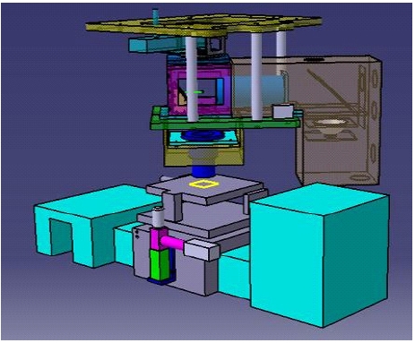
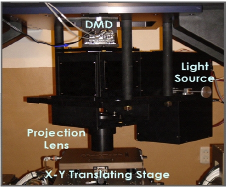
Fig. 14 shows 3D images of the collection of parts used for fabricating the maskless lithography equipment and Fig. 15 shows the system actually fabricated and installed.
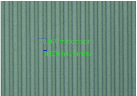
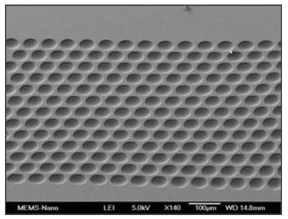
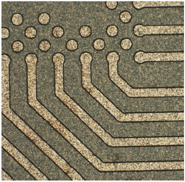
In order to verify the feasibility of the maskless lithographic optical system, lithography experiments were performed using the equipment where the developed optical system is loaded [20]. The lithography result shown in Fig. 16 is 4 μm vertical lines on a wafer and it proves that 4 μm resolution is achieved. Fig. 17 shows a microscopic image of a PCB pattern on a flexible substrate and Fig. 18 shows an electron microscopic image of a mold sample made by the developed optic system, by which an aspheric MLA can be fabricated, and in the near future it will be used for development of the maskless lithography using an aspheric MLA.
We separately designed and fabricated an illumination part, and a projection lens part, and by integrating them, we completed a 4 μm class maskless lithography optical system. This system can be applied to PCB and/or FPD fabrication, and we predict that this system could solve various problems like expense and time in fabricating the masks, contamination by masks, disposal of masks, and the alignment of masks which were major disadvantages of the conventional mask lithography optical system. The proposed system could be verified by lithography experiments which gives the line pattern with the resolution of 4 μm line width. Our future work will mainly focus on the development of the maskless lithography optical system with MLA which is developed by this equipment.