The development of the transistor and laser has significantly affected our lives through the introduction of hand-held electronic gadgets and advanced telecommunication technology. These two broad areas include many important applications in the fields of medicine, security, pollution monitoring and worldwide communication [1, 2]. Recently, a new class of light sources named the transistor laser (i.e. three terminal laser) has evolved. It incorporates the properties of both devices and has not yet been extensively explored [3]. This device tightly controls the light emission by means of the applied field through a derive gate electrode and can be integrated into modern monolithic circuits, while allowing the output optical field to be much more rapidly varied in comparison to laser diodes [4]. In the present era, the focus on security and medical applications has been increased with a particular demand for compact devices which can be achieved using monolithic solid state monochromatic coherent terahertz (THz) sources with the well-known ability of terahertz EM waves in these fields [5]. The compatibility of terahertz sources with integrated circuits has also made it possible to develop a new class of photonic chips for compact pocket based devices offering fast computing, which can boost Si based technology [6].
It must be noticed that conventional solid state sources cannot be operated in the terahertz regime, because of many physical issues and because it is impossible to integrate them with present chip technology. In the past decade, quantum cascaded lasers (QCL) and nanometer transistors have been used efficiently as solid state THz sources. A lot of prototypes of QCLs have been presented for different frequency ranges, which are limited at lower frequencies with low output powers [5, 7]. Therefore, nanometer transistors which operate on the basis of the charge plasma instability (Dyakonov-Shur theory or D-S theory) in saturation mode are gaining interest. They offer a vast tuning range in the THz frequency band by varying the applied gate voltage [8]. In addition, these devices can also be utilized as THz sensors and are free from the band gap engineering usually needed in common light sources This freedom is very difficult to achieve in the terahertz regime [9].
The first THz emission report by using a high electron mobility transistor was presented by Knap et al. based on charge plasma instability [10]. These devices have presented a wide tuning range of resonance frequency with gate voltage swing and have shown non-steady state in output current characteristics in the form of a negative differential resistance region. Many reports have been published for THz emission as well as detection using III-V group materials and Si by plasma wave nanometer transistors [11-14]. However, Gornik and Tsui have reported emission in the infrared regime by using Si inversion layers due to radiative transitions between electric subbands as well as plasma oscillations [15, 16]. Deng and Shur have also presented the possibilities for Si MOSETs as a THz emitter [17]. They have discussed different physical requirements (i.e. gate length, mobility of carriers and momentum relaxation time) for the Si active region and expected a THz emitter with sub-40 nm gate length with plasma wave instability, which helps in minimizing the attenuation of plasma oscillation. SiO2/Si/SiO2 FET structure was reported with the 0.2 ps momentum relaxation, which also set a milestone and a hope for Si based THz plasma wave transistors. Rumyantsev et al. and Meziani et al. have reported non-resonance mode THz detection by using strained-Si MODFETs [18, 19]. They have used long channel length devices (~200 nm) which were quite far from the achieving the plasma wave resonance in the Si active region as discussed by Deng and Shur. Recently, Park et al. have also presented a design guideline for a resonant THz emitter with strained-Si active region FETs based on theoretical analysis and have discussed the possibility in the THz regime [20].
In our earlier work, a simulation study has been performed successfully with Si FETs by incorporating biaxial tensile strain to test plasma wave resonance oscillations because of enhanced electron mobility [21]. This report discussed the strain induced physical process in detail with the lowering of resonance THz frequency due to the significant increase in channel charge. It must be noticed that strain reduces inter-valley scattering and enhances the carrier mobility which in-turn increases the momentum relaxation time (tm). Enhanced tm maintains the necessary condition of wtm > 1 for charge plasma oscillation, where w is the angular frequency and reduced the attenuation of the plasma wave factor (1/2tm) [22]. In other words, strain enhanced the characteristic damping length of the plasma wave, which in turn made the nanoscale strained-Si active region suitable for resonance charge plasma oscillation in the terahertz regime. Once the plasma wave was established in the strained-Si active region, it started to grow through the gain provided by the successive back and forth oscillation between the cavity boundaries of the source/drain, and it continued emitting with the resonance plasma frequency [8]. Charge plasma oscillations can be established in a real device by asymmetric boundary conditions at the source/drain boundary, which can be achieved by keeping the open circuit condition at the source and short circuit condition at the drain [22].
However, the nature of the emitted spectrum has been observed to be broadband and incoherent in the perpendicular direction of the plane of the active region [23]. This observation might be expected to be used to develop a new kind of monochromatic coherent terahertz source by incorporating an optical cavity to fill the gap of monolithic THz sources. Therefore, this study has aimed to realize a coherent monochromatic THz emission from a plasma wave strained-Si channel transistor by introducing a vertical cavity with the help of a quasi-periodic distributed Bragg reflector (DBR). To the best of our knowledge, this is a first report for a surface emission terahertz transistor as a monochromatic coherent source, which is an extension of D-S theory. The proposed device concept operating in the terahertz regime may help for realistic applications. The remaining sections of this study explain the progress of the monochromatic coherent terahertz emission produced by strained-Si channel MOSFETs by the combination of strain engineering and charge plasma instability.
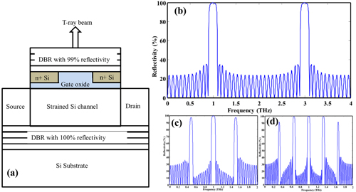
The proposed device block diagram is shown in Fig. 1(a) by incorporating a vertical cavity designed by DBR into the basic device structure reported in ref [21] with split gate. The proposed device is based on resonance charge plasma oscillation which takes place between the source and drain boundary cavity with asymmetric boundary conditions as discussed in the introduction section. However the conventional laser works on the stimulated emission with a certain threshold. A similarly proposed device concept of resonant charge plasma oscillation was also established with a certain threshold voltage and further, photonics oscillation started to grow in the vertical cavity. The proposed device used two cavities to emit monochromatic coherent output in the THz regime with the help of plasma wave stimulation emission. Therefore, the proposed device concept can also be called terahertz amplification by plasma emission of radiation.
Furthermore, device dimensions should make the quality factor for the plasma wave cavity (stm / Lg) should be greater than 10, where s and Lg are plasma wave velocity and gate length, and gate width (Wg) should be asymmetric with gate length which plays the major role to achieve instability or Wg / Lg ~ 100 [22]. The thickness of the active region is kept below the critical thickness to avoid strain relaxation. The vertical cavity is basically used to achieve the wavelength selectivity with high quality factor from the broad emission, as usually used in a VCSEL. The two DBR (one of 100% and other of 99% reflectivity) have been designed with multiple period of alternating layers of high and low refractive index layer for tuning the desired reflectivity. For the THz regime, an SiO/SiO2 material pair (index ratio~1.2) has been selected. Figures 1(b)-1(d) shows the reflectivity of DBR with periodic and quasi-periodic sequence of high and low index. Maximum reflectivity occurs at odd multiples of the resonance frequency and thickness of the layer is kept equal to a quarter of the wavelength. Figure 1(b) shows the reflectivity pattern for a periodic DBR with alternative low and high index layer (say LH) for 1THz resonance frequency which uses quite broad peaks with 8 periods to achieve 100% reflectivity. Further Figs. 1(c) and (d) shows the reflectivity patterns for quasi-periodic DBR for the same resonance frequency and reflectivity. Quasi-periodic sequence has been achieved by replacing one low index layer by a high index layer from the two consecutive LH periods. Then the new sequence period will have one low index and three high index layers (say L(3H)) [24]. Reflectivity of the new quasi-periodic DBR with 8 periods is shown in Fig. 1(b), which shows the much reduced bandwidth with two side reflectivity peaks around the central peaks. Similarly, a new quasi-periodic sequence is designed by replacing two low index layers with the high index layer from the three consecutive periods of periodic sequence that results in a quasi-periodic sequence of “L(5H)” type. Reflectivity of this quasi-periodic sequence is shown in Fig. 1(d). A more closely spaced number of reflectivity peaks have been observed with more reduced bandwidth. The quasi-periodic DBR has found more effective for finely tuned resonance frequency with lower bandwidth. Therefore, quasi-periodic sequence DBR was implemented with the proposed device in place of a periodic sequence to design the vertical optical cavity. This unique property of the quasi-periodic structure can help to design a multi-color output with a single device design.
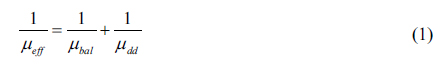
This section presents the simulation results for the proposed terahertz transistor designed on a strained-Si-on-insulator substrate based on charge plasma oscillation by using the ATLAS device simulator. The physical process of enhanced momentum relaxation time is discussed in our earlier work which modifies the effective mobility with the rate of momentum relaxation by hopping of energetic/hot carriers. The study is performed with 25 nm gate length with 2 mm gate width and 1.8% strain in silicon for the device. In this proposed structure, the strain is assumed to be introduced in the ultrathin Si layer over the SiO2 by the layer transfer technique [25] over epitaxial grown DBR on Si substrate. The momentum relaxation time (eμeff / m) value 1 ps is achieved: where, e, μeff and m are the electronic charge, effective mobility and effective mass in the strained-Si active region. Effective drift-diffusion mobility (μdd) has considered phonon scattering, surface roughness scattering and coulomb/ionic scattering mechanisms for better physical insight. Along with it, ballistic mobility (μbal) is also considered because of increased ballistic efficiency in nanoscale strained channel FETs as follows [26, 27]:
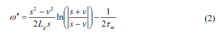
Plasma wave growth factor (ω") is also an important parameter which controls the growth of oscillation and has to be maintained greater than zero for all operating frequencies of the device as follows [8]:
where, ν is the electron fluid velocity. s and ν can be estimated by the formula and ν = Ids /(ensWg). Vgs, Vth, Ids and ns are the gate to source voltage, device threshold voltage, saturation drain current and sheet charge density, respectively. Vgs − Vth is termed as gate voltage swing.
The first term in the expression denotes plasma wave increment and the second term is related to attenuation of the plasma wave. The second term is inversely proportional to momentum relaxation time, which reduces significantly with increasing strain. Therefore, strain channels have to have the capability to overcome attenuation of the plasma wave and enhances the probability of resonance. It has to be noticed that plasma wave instability is a phenomenon governed by perturbation of charge density with respect to time and space (derived by hydrodynamic Euler Eq. and continuity Eq. [8]) as follows:
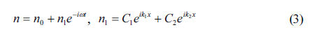
where, n0 = Cox (Vgs − Vth) / e and n represents temporal and special perturbation of charge density. C1 and C2 are perturbation coefficients. k1 and k2 are corresponding wave vectors [8]. Therefore, instability can be established at low charge density by keeping s > ν for the device operation at low gate voltage swing, which also helps in minimizing the scattering mechanism and results the increment in effective mobility. As the above velocity relation established with the increase in gate voltage swing, the reflection coefficient (s − ν / s + ν) of drain/channel boundary become +ve and starts to reflect charge carriers. This phenomenon creates the accumulation of charges in the active region. According to the Fermi-Dirac statistics, ν increases with increase in charge carrier density in channel along with s for 2D degenerate electron gas which plays a significant role in the strong inversion operated terahertz transistor emitter [20]. Therefore, the Fermi model has been used for the Fermi-Dirac carrier statistics along with the hydrodynamic model to simulate the motion of electron fluid in the channel. Such nanoscale strained-Si channel FETs with low threshold voltage and high velocity overshoot effect can be operated in the diffusive or quasi- ballistic mode by optimizing operating conditions. Thus drift velocity order should be in the same order of plasma wave velocity, which is a major requirement to achieve plasma emission in THz regime [10]. Same order of both velocities also favors to keep the Mac number (ν / s) between 0 and 1 to strengthen the THz emission. The non-steady state operation of the device results in the fluctuation in effective mobility with the momentum relaxation time (tm). Hence, transient behavior of mobility and accumulation of charge in the active region is responsible for this non-steady state of conduction from which arises plasma wave instability. To analyze actual device behavior, the physical effects of accumulation of charge and transient mobility are added to the ATLAS simulator library by using C-Interpreter.
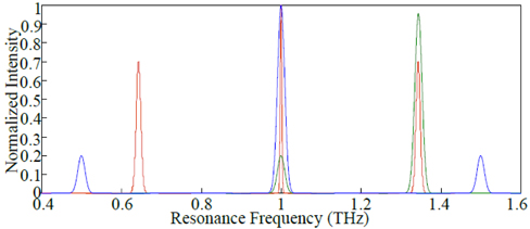
In view of the above, the output spectrum of a device with different DBR of reflectivity is shown in Figs. 1(c) and (d) and operating conditions are shown in Fig. 2. The blue line spectrum represents the DBR reflectivity shown in Fig. 1(c) which results in one central peak with two broader week peaks. The central peak at 1 THz is related to the resonance frequency of the cavity and other two weak peaks at 0.5 & 1.35 THz are related to the tail spectrum around the central resonance frequency corresponding to the lower reflectivity peak shown in Fig. 1(c) around the resonance frequency. No resonance emission is observed below 1 THz frequency. Further, the resonance frequency is shifted from 1 to 1.35 THz by decreasing the drain to source voltage (Vds) with the same DBR system as can be seen by the green line spectrum because of the increase in effective threshold for the charge plasma oscillation. This phenomenon resembles the lower strain which also supports the higher resonance mode of plasma frequency [21]. Numerically, it can be explained in terms of increment of difference between plasma wave velocity and drift velocity, which leads to the increment in resonance frequency as follows:
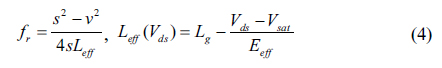
where, Vsat is the source-drain saturation voltage, Leff is the effective channel length and Eeff is the effective electric field. The sheet charge density found to be approximately 3.8×1011 cm-2 with plasma wave velocity and drift velocity equal to 2.1×107 cm/s and 1.9×107 cm/s respectively, which supports the 1 THz resonance frequency. To show the versatility of quasi-periodic DBR, the output spectrum is also plotted with that of another system with reflectance shown in Fig. 1(d) for fine tuning of resonance frequency and multi-color operation. It can be seen from the red line spectrum in Fig. 2 with 1 THz resonance frequency that two equally spaced slightly lower intensities at 0.65 & 1.35 THz peak around a central peak at 1 THz are observed. These side peaks also become strong as the central peak because of the very closely spaced reflectance peak shown in Fig. 1(d) and supports the optical resonance for frequencies in close proximity of the central resonance frequency. The bandwidth of 1 THz frequency is found to be much less than the side peak because of lesser dielectric losses. This spectrum approves the multi-color operation of the proposed device. It has to be noticed that a similar spectrum can also be achieved by a periodic design of the DBR by using two different sizes of optical cavity in a single device, which makes the device bulky with ensuing complications. However, in the proposed device, optical resonance for multiple frequencies can be achieved by just changing the DBR. It is also realized that the spectrum corresponds to a second set of DBR systems that shows a much sharper peak. So the quasi-periodic DBR cavity with the greater number of periods is found more effective for tuning of resonance frequency along with reduced linewidth. The proposed device also has functionality to tune the resonance frequency by strain towards lower harmonics [21].
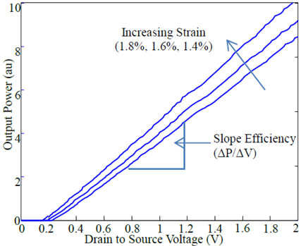
For a monochromatic coherent source, output power and emission efficiency have to be optimized to enhance their applicability, which are the most important parameters for designing a device. Plot for output power with respect to drain to source voltage (Vds) for different value of strain is shown in Fig. 3. Output power is found to be increased with increasing Vds because of the strengthening of the charge plasma instability in the active region. Further, emitted power gets enhanced with the increment in strain because of increase in momentum relaxation time, which in turn increases the charge accumulation in the channel and improves the growth of the plasma wave. The emission threshold below which there will be no emission, decreased with strain;. Therefore, two threshold values exist for the terahertz emission: one is related to the gate voltage and the other to the drain voltage. Generally, emission efficiency can be explained by the external quantum efficiency, which is defined as the number of emitted photons with respect to the injected number of electrons. However, THz transistor devices are controlled by terminal voltages and conventional definition is not well suited for them. Therefore, the slope efficiency has preferred here to calculate by the formula shown in figure for the proposed device. The calculated slope efficiency found to be enhanced with the increasing strain. It is increased to 33% with the 0.4% increase in strain. This might be caused by the decrease in the effective threshold voltage of the device, which reduces gate voltage swing required to achieve the minimum charge density responsible for the efficient terahertz emission.
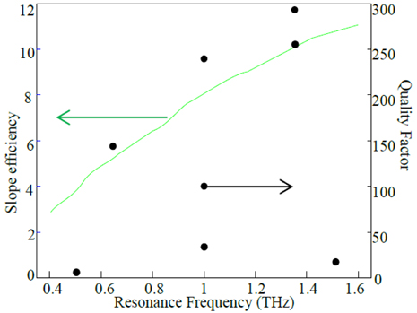
A significant parameter of the vertical optical resonator is quality factor, which represents the optical losses in one round trip and bandwidth of the resonance frequency. Therefore, the variation of the quality factor and slope efficiency with respect to the resonance frequency is plotted in Fig. 4. Tuning of the resonance frequency is achieved by varying the drain to source voltage. The slope efficiency has been observed to be decreased with decreasing resonance frequency, because of the lowering of the effective charge density in the active region.
It has already been discussed that higher strain in the active region enhances the ωτm factor in spite of supporting the lower order harmonic of the resonance frequency. However, the slope efficiency is found slight low beyond the expectation due to dielectric losses. Therefore, highly strained active medium is desirable to compensate the loss of emission efficiency. Quality factor is also plotted in this figure and found to decrease with resonance frequency. It calculated by the numerical formula f / Δf, where f is the resonance frequency and Δf is corresponding bandwidth. Wide range of Q-factor variation from 5 to 290 shows the wide applicability of the quasi-periodic DBR resonator. It can be tuned to a particular frequency by simply changing the optical thickness of the dielectric layer or index sequence. Multiple values of quality factor are estimated corresponding to a single frequency because of the dependency on the bandwidth. Bandwidth depends on whether the oscillating frequency has been matched with the reflectance peak or not. So, the highest quality factor for a particular emission frequency can be achieved by adjusting the charge plasma resonance frequency corresponding to the maxima of the reflectance pattern of the optical resonator by varying the gate and drain voltages.
Study of transient response of the proposed device is also necessary to test the ability for optical communication systems, where the applied voltage/current is modulated at several gigahertz with the steady state operation. It is necessary to ascertain the extent to which the emitter device responds to closely spaced modulation pulses. Therefore, the optical output pattern of the proposed device with respect to time is plotted in Fig. 5. A steady state oscillation in the photon density has been observed against the time of picoseconds order. This result confirms usefulness for high-speed device modulation and energy-efficient data transfer capability. These unique physics based devices have the ability to be commercialized using system on chip technology.
The proposed strain induced charge oscillation based device could pave the way towards the development of an efficient monochromatic coherent terahertz emitter. This three terminal device provides strength to control the bandwidth of the surface emission with implementation of quasi-periodic DBR which also helps to achieve multi-color emission. Further, wide range of optical resonance can be achieved for THz frequencies by customizing by different index sequence DBR. The quality factor and emission efficiency can also be tuned as per desired value for particular application. Finally, the development of quasi- periodic DBR resonator based terahertz transistor represents a milestone in the search for solid state monolithic terahertz sources. It might stimulate the search for other novel optoelectronic devices in the field of “Teratronics” involving the use of light, which is referred to as “Opto-Teratronics”.


![(a) Block diagram of proposed device structure of plasma wave terahertz transistor, (b) Reflectance of periodic DBR of [LH] type, (c) Reflectance of quasi-periodic DBR of [L(3H)] type, (d) Reflectance of quasi-periodic DBR of [L(5H)] type. The upper mirror has been designed for 99% reflectivity with five periods.](http://oak.go.kr/repository/journal/21631/KGHHD@_2017_v1n5_544_f001.jpg)