We present experimental demonstrations of electromagnetic bandgap (EBG) structures for the wideband suppression of radiated emissions from a power bus in high-speed printed circuit boards (PCBs). In most of the PCB designs, a parallel plate waveguide (PPW) structure is employed for a power bus. This structure significantly produces the wideband-radiated emissions resulting from parallel plate modes. To suppress the parallel plate modes in the wideband frequency range, the power buses based on the electromagnetic bandgap structure with a defected ground structure (DGS) are presented. DGSs are applied to a metal plane that is connected to a rectangular EBG patch by using a via structure. The use of the DGS increases the characteristic impedance value of a unit cell, thereby substantially improving the suppression bandwidth of the radiated emissions. It is experimentally demonstrated that the DGS–EBG structure significantly mitigates the radiated emissions over the frequency range of 0.5 GHz to 2 GHz as compared to the PPW.
In modern electronics, the circuit switching speed and the data rate for input/output interfaces are continuously increased. The high-speed signal of modern electronics results in wideband spectra spanning a frequency of several gigahertz (GHz). A wideband signal propagates through circuit structures embedded in printed circuit boards (PCBs), which induces electromagnetic radiated emissions in a wideband frequency range. The radiated emissions from high-speed PCBs are coupled to other devices and produce electromagnetic noises. These noises significantly degrade the system performance.
The power bus structure in PCBs is the main source of electromagnetic radiated emissions. To analyze the principle of a radiated emission and estimate the amount of the radiated emissions from a power bus, numerous theories and modeling methods are presented in [1-5]. In particular, a number of studies have focused on a parallel plate waveguide (PPW) structure for a power bus because it is typically used in PCB applications [6-8].
A PPW structure consists of two metal layers and a dielectric material located between the metal layers. One metal layer is used as the direct current (DC) power supply, and the other is used as the circuit ground. The two metals are isolated by using a dielectric material so that they do not have a DC connection between them. A boundary of the PPW structure interfaces with air or a dielectric material. Even though the shape of this structure is not limitation, a rectangular PPW is adopted frequently because of its simple design.
Further, signal excitation in the PPW produces resonant modes or parallel plate modes [9]. The parallel plate modes are excited and induce a high-voltage noise when they are driven by a signal whose frequency corresponds to the frequency of the resonant modes. In addition, an electrical noise is easily radiated. In the resonant modes, the radiated emission of the PPW is similar to that of a planar patch antenna with a small, finite ground plane.
To solve the radiated noise problem of a PPW-based power bus, methods for the suppression of the parallel plate modes have been studied. In particular, numerous studies have been conducted on electromagnetic bandgap (EBG) structures [10-14]. The EBG structures suppress the parallel plate modes in the wideband frequency range. An EBG structure using defected ground structures (DGSs) mitigates the resonant modes in a frequency range wider than that considered in conventional methods. A DGS–EBG structure achieves the wideband suppression without the use of additional materials and expensive methods. The advantages of the DGS–EBG structure are described clearly in [12]. However, its radiated emission characteristic has not been discussed.
In this study, we experimentally demonstrate the electromagnetic radiated emission characteristics of the DGS–EBG structure. We design the new test vehicle whose low cut-off frequency value for a fundamental stopband is <1 GHz because we consider PCB applications in which the spectra of the simultaneous switching noise are arranged in frequencies around 1 GHz. This study contributes to the experimental demonstrations of the DGS–EBG structure suppressing the radiated emissions in the wideband frequency range.
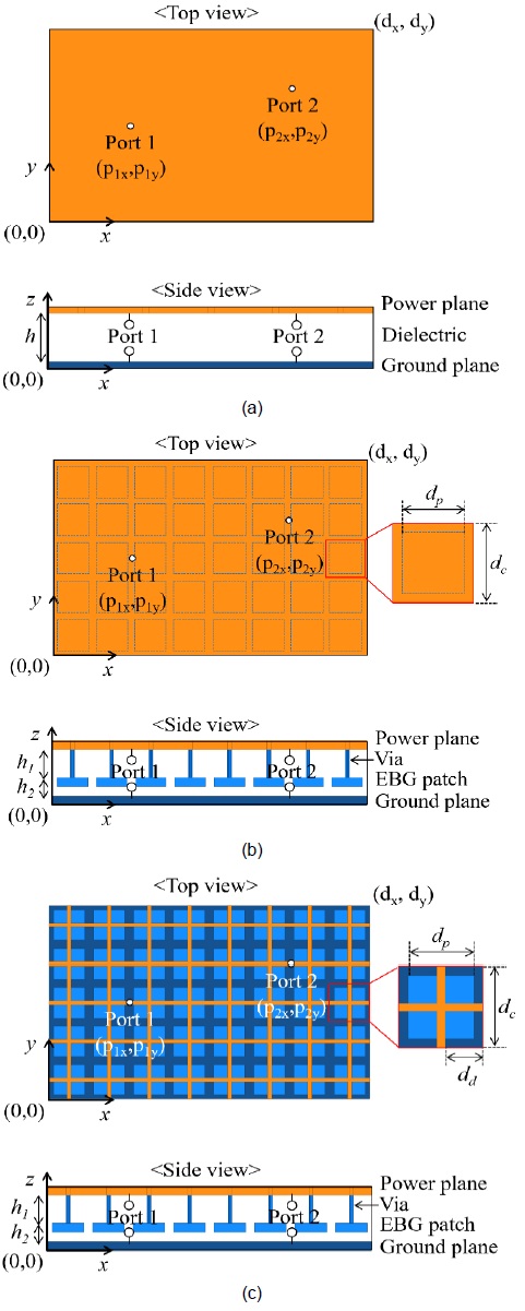
In this section, three test vehicles are designed to experimentally demonstrate the radiated emission characteristics of a power bus using a DGS–EBG structure. As shown in Fig. 1, we design a PPW-based power bus, a power bus using a mushroom-type EBG (M-EBG) structure, and a power bus using a DGS–EBG structure. The PPW-based power bus in Fig. 1(a) is a rectangular PPW structure consisting of a power plane and a ground plane. The distance between the two planes is
The M-EBG structure is presented in [10] to suppress the resonant modes in the rectangular PPW structure. It consists of three layers, namely a power plane, a patch, and a ground plane. Rectangular patches are arranged periodically on the board. The power plane is connected to the patch with a via structure.
The distance between the power plane and the patch is
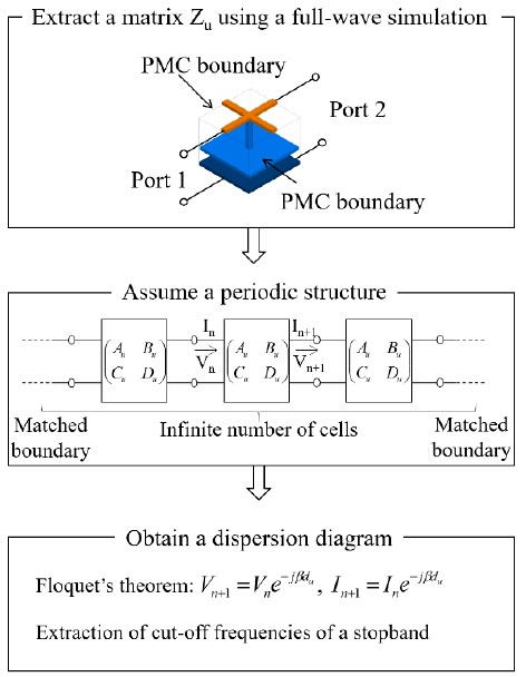
For the DGS–EBG structure newly designed herein, a dispersion analysis is performed. The procedure for this analysis is presented in Fig. 2. In the first step, a unit cell structure is defined. Using a full-wave simulation based on the finite element method (FEM), the network parameter of the unit cell structure is extracted. The network parameter is converted into an ABCD matrix. We assume a one-dimensional periodic arrangement of the DGS–EBG unit cell. The infinite number of unit cells and the perfectly matched boundary are assumed. By applying the Floquet–Bloch theorem [9], we can extract the relationship between the voltages and the currents of port 1 and port 2, which is equal to the impedance matrices. The unit cell structure is equivalently modeled as a transmission line circuit with a characteristic impedance of

The design variables are shown in Fig. 1. For the dispersion analysis, the corresponding dimensions are presented in Table 1. The dimensions of the power buses are determined in order to form a stopband of the DGS–EBG structure around 1 GHz.
[Table 1.] Dimensions and design variables for the dispersion analysis of a DGS?EBG structure
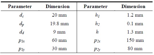
Dimensions and design variables for the dispersion analysis of a DGS?EBG structure
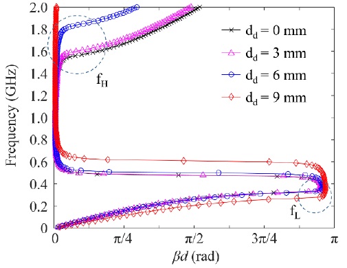
To examine the DGS effect, the size
The low cut-off frequency is shifted down as the DGS size is substantially increased. The high cut-off frequency is significantly increased as the DGS size increases. The fH value for the DGS size of 9 mm is more than 2 GHz, whereas the
[Table 2.] Cut-off frequencies of a stopband with respect to various DGS lengths
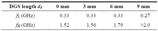
Cut-off frequencies of a stopband with respect to various DGS lengths
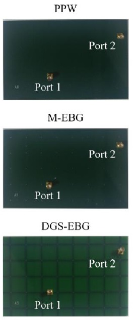
We fabricate three test vehicles by using a commercial PCB process, as shown in Fig. 4. In the PCB process, copper is used for the metal layers and FR-4 is used as the dielectric material. The through-hole via technology is used for connecting between a power plane and a patch. The board size (i.e.,
1) Noise Coupling Coefficients
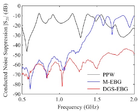
Noise coupling coefficients are measured to verify the design of the DGS–EBG structure before measuring the radiated emission characteristics. The scattering parameters between port 1 and port 2 are measured using a vector network analyzer. Fig. 5 shows the measurements of the noise coupling coefficients of three test vehicles. We observed that the PPW-based power bus has high noise coupling coefficients because of the parallel plate modes. The M-EBG structure mitigates the parallel plate modes. However, the M-EBG structure fails to suppress the resonant modes over the frequency range starting from 1.5 GHz. In contrast, the DGS–EBG structure suppresses the resonant modes in the wideband frequency range of 0.5 GHz to 2 GHz, which is expected from the dispersion analysis.
2) Radiated Emissions
The radiated emission characteristics of the three test vehicles are measured using a reverberation chamber [15] and a vector network analyzer. The reverberation chamber introduced in [15] has the advantage of capturing the radiated emission characteristics for the PCB boards, which shows various directivities with respect to the resonant modes. Port 1 of the vector network analyzer is connected to either port 1 or port 2 of the test vehicle. Port 2 of the vector network analyzer is connected to a receive antenna. Both the test vehicle and the receive antenna are placed in the working volume. During the test, two stirrers are rotated to obtain a uniform field statistically. The method for measuring the radiated emissions by using a reverberation chamber is described in [15].
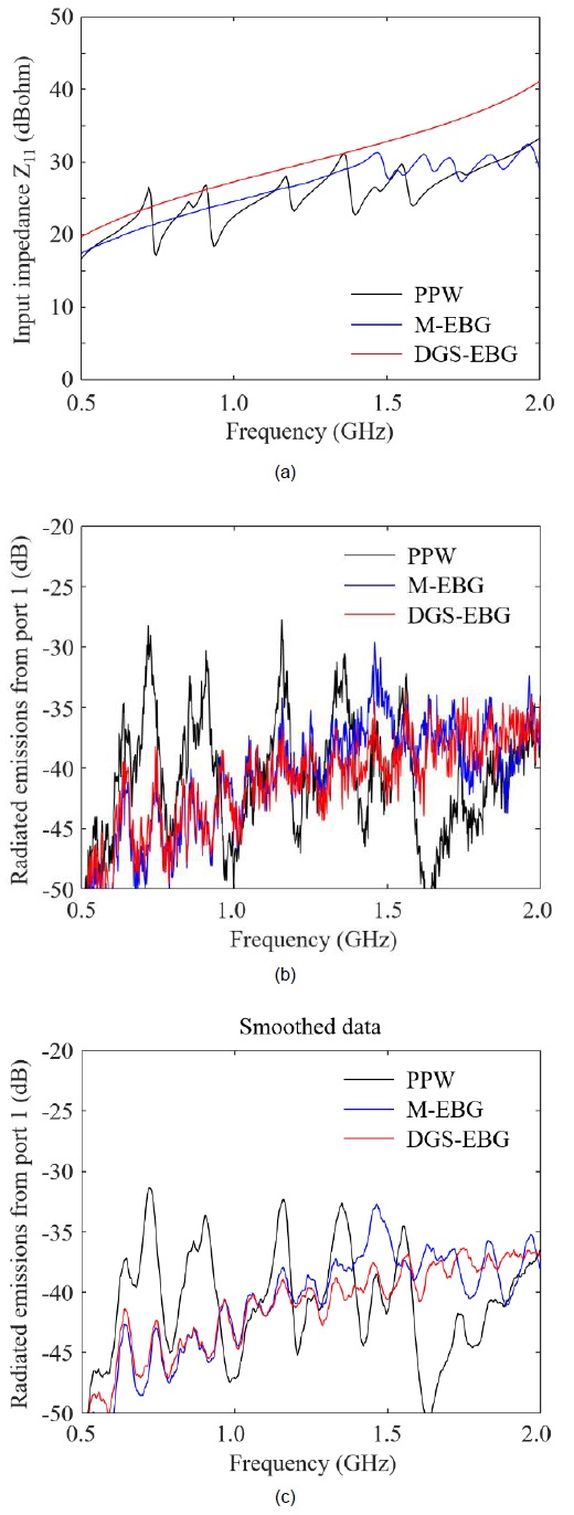
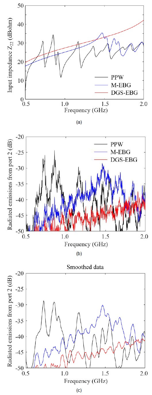
Figs. 6 and 7 depict the measurements of the input impedances, radiated emissions, and smoothed radiated emissions for port 1 and port 2, respectively. Fig. 6(a) shows the input impedances measured at port 1 of the three test vehicles. The PPW-based power bus has a number of resonant modes, and the M-EBG power bus has the resonant modes above the frequency of 1.5 GHz. In contrast, the DSG–EBG power bus suppresses the resonant modes in the wideband frequency range of 0.5 GHz to 2.0 GHz. This result is also expected in the dispersion analysis.
Similar results are observed in the measurements of the radiated emission characteristics shown in Fig. 6(b). The PPW-based power bus shows a high level of radiated emissions induced by the resonant modes. For the M-EBG power bus, the peak of the radiated emission is shown at the frequency of 1.5 GHz. However, the DGS–EBG power bus substantially suppresses the radiated emission peaks. For port 2, the measurement results are the same as those for port 1. Consequently, through the measurements, we clearly demonstrate that the DGS–EBG power bus suppresses the radiated emission in the wideband frequency range.
The radiated emission characteristics of the DGS–EBG power bus are experimentally demonstrated. The dispersion analysis based on a unit cell model with a full-wave simulation is presented for the design of the DGS–EBG structure. The experimental results prove that the radiated emissions from the DGS–EBG power bus are improved as compared to the conventional methods because the DGS–EBG power bus significantly suppresses the resonant modes over the wideband frequency range of 0.5 GHz to 2.0 GHz.