Recently, many mobile devices including smart phones require an efficient regulator to prolong battery life. Among the various regulators available, the Low Dropout Regulator (LDO) has the advantage of small ripple and low noise [1-3]. Other switching-type regulators [4,5] have their own advantages such as wide operating current ranges and high frequency operation, but their conversion efficiency changes significantly with variations in load resistance. Furthermore, their feedback block for a fast dynamic response requires many additional circuits, which occupy a large-die area in an integrated circuit (IC).
Advantages of the LDO regulator is that it provides low-noise and accurate output voltage with a relatively simple circuit, which is composed of an op-amp, transistor, and feedback voltage divider. The characteristics of the line and load regulations are mostly dependent on the transistor and the output capacitor. Conventional LDOs usually have a large-sized output capacitor for stability. Most of the LDO performance is greatly affected by the large output capacitance. The large-size off-chip capacitor can be a major drawback for fully integrating LDO and for chip minimization. Recently, capacitorless LDO regulators were proposed involving compensation or the capacitor coupling effect. Our aim is to develop a small-sized capacitor-less LDO with a fast transient response by applying a single-stage compensator.
Many electronic systems incorporate some form of feedback. The advantages of feedback [6] include reducing the effects of noise and nonlinear distortion, that is, minimizing the contributions to the output of unwanted electronic signals generated by circuit components. A simple method of frequency compensation consists of introducing a new pole in the circuit system at a sufficiently low frequency.
In order to reduce large-sized output capacitance, many structures for Miller compensation have been proposed, as it provides pole-splitting compensation, which can result in increased bandwidth and fast transient times. Currently, nested Miller compensation (NMC) usually applies multiple gain stages that are bypassed by a capacitor [7-10]. Because of the Miller compensation, the compensating capacitance will be multiplied by the stage gain, resulting in a much larger effective capacitance. Furthermore, a much wider bandwidth for the amplifier can be obtained because of pole splitting. The multiple-stages and capacitors in LDO eventually provide a large-sized die-area in IC, although the regulator can be sufficiently controlled by the compensator. Our aim is to use a single-stage and R-C compensator in LDO. The electrical characteristics of the LDO can be regulated by the parameters of the stage and the compensator.
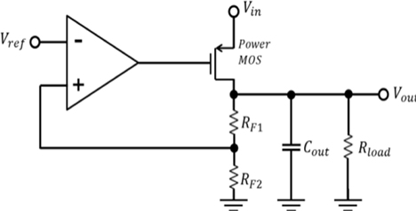
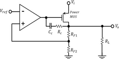
The conventional LDO structure is shown in Fig. 1, which includes an op-amplifier, power MOS, voltage divider, and large sized micro-farad capacitor. Power MOS is for the large current. In the CMOS integrated circuit (IC), which requires chip-minimization for high performance, a large sized capacitor in the output stage of LDO is not recommended and variable capacitance can provide more stable operation in the frequency response. Many works have been proposed to develop a capacitor-less LDO topology in the output stage.
In this work, resistance-capacitance (R-C) compensation is proposed to obtain a small-sized LDO with a fast transient response. The feedback R-C compensation is connected between the gain-stage and the power MOS in LDO. The resistor and capacitor in the feedback are supposed to provide additional pole and zero in the frequency response. The R-C compensation includes only a single gain-stage to obtain a stable frequency response. An additional zero beside the pole-splitting can be applied to increase the phase margin. The integrated circuit (IC) for the LDO is obtained with the 0.35 μm CMOS process. Simulation of the LDO is performed in terms of the switching characteristics of the load and line regulation and the frequency response.
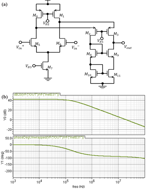
The circuit of an error amplifier for LDO is shown in Fig. 2(a), and the Bode plot for the frequency response is in Fig. 2(b). The differential pair in an error amplifier uses dc-biased current sources for a large current driving capability.
The frequency response for the Bode magnitude and phase plots indicates that the phase margin is about 80o, with a magnitude of 40 dB, which means a stable frequency response. The effect of a single pole due to an output capacitance is shown in the frequency response. When this amplifier is employed in the LDO for the regulator, the frequency response can be unstable because of a decrease in the equivalent resistance from the MOS switch and feedback resistor.
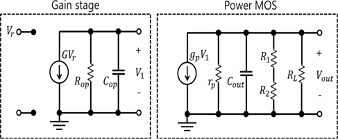
The equivalent small-signal model for the conventional LDO is shown in Fig. 3. It is composed of two blocks for the gain-stage and the power MOS. The gain-stage is the small-signal model of the op-amp and includes the resistor Rop and capacitor Cop, while the power MOS block includes the output capacitance Co, feedback resistors R1 and R2, MOS output resistance rp, and load resistance RL. The conductance values for the gain stage and power MOS transistor are expressed as G and gp. The frequency response and stability can be obtained from the loop gain, poles, and zeros. In the small- signal circuit, the outputs of gain and LDO, V1 and Vout, are given by
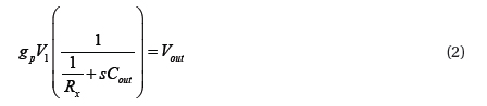
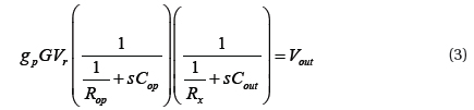
, where Rx is the equivalent parallel resistance that includes the feedback resistors RF1 and RF2 and MOS output resistance rp. Multiplication of equations (1) and (2) with elimination of V1 can be performed to give the following (3),
, therefore, the loop gain is expressed as
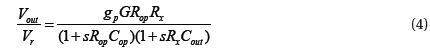
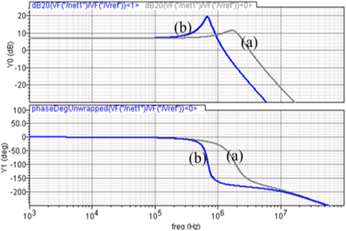
The gain loop has two poles of (RopCop)-1 and (RxCout)-1, which come from the capacitances from the gain stage and the power MOS including the output capacitance. When the two poles are almost equal, the slope in the Bode plot provides -40 dB/decade from the cutoff frequency.
Our results in the Bode magnitude plot shown in Fig. 4 (a) and (b) indicate a slope of -40 dB/decade at the cutoff frequency of 2 (0.7) MHz obtained at the output capacitance Cout of 10 (100) pF. The conventional output capacitance is about 100 pF, which is relatively large for integration into the system-on-chip design. Both of the phase margins are under 20o, which means an unstable frequency response. In a stable system, the phase margin should be over 60o.
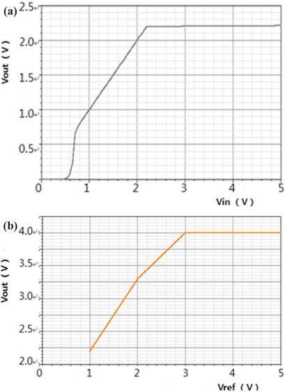
The conventional LDO regulator uses a large load capacitor for the stability requirement and load transient response. The large load capacitor in the LDO regulator provides the dominant pole and stores energy for the output voltage. A capacitor-less LDO has the advantage of fast transient response in addition to a stable frequency response if it has a proper compensator and gain stages. The transfer characteristic, represented as the output Vout with variation of the input voltage Vin, is shown in Fig. 5 (a). As long as the input voltage Vin is larger than 2.2 V, the output voltage Vout is close to 2.2 V, which can be obtained easily with the variation of the feedback and reference voltages. Other values of Vout can be obtained with the variation of the feedback resistors RF1 and RF2 in Fig. 1. Fig. 5(b) shows the output voltage with an increase of the reference voltage Vref and the slope, which depends on the resistors RF1 and RF2. The expected output voltage is obtained. In this work, the load and line regulation of the conventional LDO are well controlled within a few micro-seconds as will be shown later. A short transient time for the regulator can be obtained with the proper selection of a reference voltage Vref and the ratio of two resistors RF1 and RF2.
A nested Miller compensation (NMC) is introduced as an effective way to compensate an amplifier. The NMC structure usually includes multipath input stages connected in parallel with the main amplifier. Although the pole-splitting in the NMC structure can be obtained by the corresponding capacitors, configuration of the proper parameters to obtain a stable system is difficult. Furthermore, multiple gain-stages require a large diearea and power consumption. Our work proposes R-C compensation as shown in Fig. 6. In the feedback circuit between the gain-stage and power MOS, the resistor is connected in series with the capacitor in order to generate zero and pole in the frequency response.
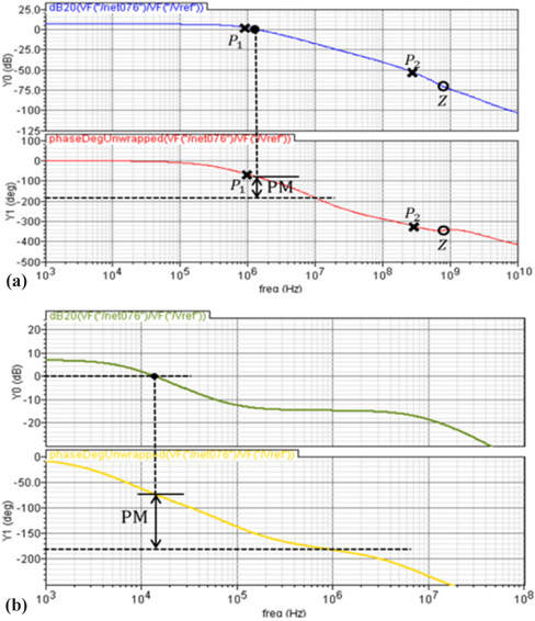
Figure 7 is the Bode plot applied for the frequency response of the proposed LDO. Fig. 7(a), which is the result at Cc = 10 pF, shows the two-pole and single zero. In the conventional LDO, the dominant single pole appears because of the large output capacitor. The compensating R-C element can cause the unity gain to be located at a lower frequency and causes the phase margin to increase. The parameter values in the compensating circuit introduce the compensating frequency and produce a more stable frequency response. On the other hand, in conventional LDO, the dominant pole frequency comes from the large output capacitor, which can produce large transient times. The advantage of the proposed LDO is that it uses only a single compensation in a single gain-stage, which can reduce the die-area and power consumption significantly.
Without compensation, the phase margin in Fig. 3 is within 20o. However, with R-C compensation as shown in Fig. 7(a), the zero Z is included in the two poles P1 and P2. Fig. 7(a) shows that the phase margin increases to 100o. The stability is much better. The R-C compensator produces two widely-spaced poles and a zero. The dominant pole P1 is much lower than the other pole P2. Fig. 7(b) is the result of the phase margin when the compensating capacitance Cc is 1,000 pF. The zero Z is located between the two poles. The phase margin is about 107o. The location of the zero is important to improve the stability in the frequency response and to increase the phase margin.
Compared to the other reported compensation, which includes a single capacitance or multiple feedback stages in LDO, the proposed R-C compensation provides much easier manipulation of the compensating parameters to find the proper pole and the zero. In this circuit, a small number of circuit parameters can decide the location of the zero and phase margin. In the conventional LDO, the multiple parameters of the gain stage, power MOS, and the output capacitance cause difficulty with finding the proper values for a stable system. The transient time during the on-off switching can be significantly reduced by the proposed compensation.
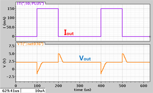
The characteristics of line and load regulation in the proposed LDO are shown in Fig. 8 and 9, respectively. In the line regulation, switching input voltages of 5 and 2.5 V are applied, whereas in the load regulation, the output current Iout of 150 mA is applied for a high logic state. High performance for line and load regulations is obtained in the 0.35 μm CMOS simulation test.
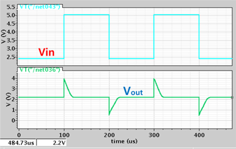
Figure 10 shows the line transient response with input voltage switching from 5 to 2.5 V, where (a) and (b) are the results for the conventional LDO with Cout = 100 pF and for the proposed LDO with Cc = 10 pF, respectively. The transient time in (a) and (b) are 32 and 2.8 μs, respectively. The ratio of the line regulation in (a) is 0.7%/V, while that of (b) is under 0.01%/V. The proposed LDO shows excellent line regulation with a low transient switching time of 2.8 μs resulting from the low feedback capacitance Cc in the R-C compensation.
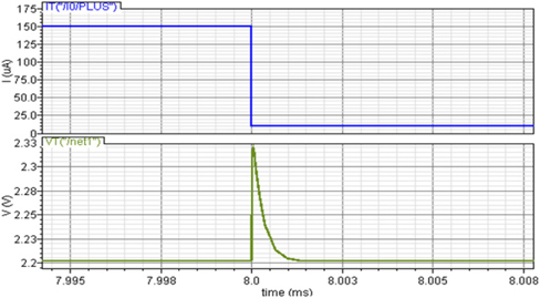
The load regulation of the proposed LDO is shown in Fig. 11, in which the input current is switched from 150 to 0.1 μA. The output voltage before and after the switch is almost the same, close to 2.21 V. The transient time is 0.8 μs. The result also shows excellent load regulation with a low transient time within 1 μs.
The effect of the compensating capacitance Cc in the proposed LDO is studied in terms of the phase margin and transient time.
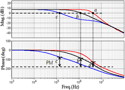
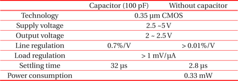
Figure 12 shows the variation of the phase margin with the change of the capacitance Cc. The variation of the capacitance Cc by 1 pF, 10 pF, and 100 pF, is indicated as a, b, and c. The phase margin shows an increase with the increase of Cc. More stability comes with higher compensating capacitance. The switching transient time is supposed to increase with larger capacitance. EMI (electromagnetic interface) noise can be reduced because of the larger transient time, not because of the peak switching voltage. This result implies the dependency of EMI noise on the compensating capacitance, which also affects the stability of the frequency response. In the line regulation, which affects the input voltages, the noise factors can be both the peak switching voltage and the frequency. However, the switching voltages appear to be the same with variations in the compensating capacitance. The performance summary for the conventional and proposed LDOs is in table I, which shows that the conventional LDO has the output capacitor of 100 pF, while the proposed LDO has no output capacitor. The proposed LDO shows line regulation under 0.01%/V and significantly reduces the transient time to be about 2.8 μs, which is much better performance compared tothan the conventional LDO.
[Table 1.] Performance summary.

Performance summary.
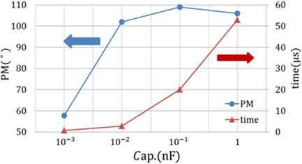
The phase margin and transient time are obtained at the resistance Rc of 0.5 kΩ, with line regulation when the input voltage changes from 5 V to 2.5 V.
Figure 13 shows that the transient time increases with the increase of the compensating capacitance Cc. The phase margins are saturated at about 105o. At the compensating capacitance Cc of 0.1 nF, the phase margin and transient time are determined to be 109o and 20 μs, respectively. The results indicate a stable frequency response.
A resistor-capacitor (R-C) compensation is introduced in an integrated CMOS LDO in order to obtain a capacitor-free regulator with fast transient time and a stable frequency response. The elimination of large-sized output capacitors is essential for the minimization of integrated circuits (IC). The proposed LDO circuit is composed of a single gain-stage and R-C compensator. The frequency response of the proposed LDO has two widely spaced poles and a zero. The phase-margin is increased over 100o and the transient time is under 3 μs with the application of the R-C compensator. In the conventional LDO with Cout = 100 pF, the phase-margin is found to be within 20o, which means an unstable frequency response. Furthermore, the transient time during switching is over 30 μs. The proposed LDO is designed with the 0.18 μm CMOS process. Simulation shows that the line regulation of the proposed LDO is below 0.01%/V and the power consumption is 0.33 mW.