RF MEMS switches play a very crucial role in the rapid development of communication systems. They have tremendous applications in areas such as defense, radar, and satellite communications [1]. MEMS switches are highly advantageous due to their low loss, high isolation, high linearity, low power consumption, and ease of integration compared to conventional PIN and field effect transistor (FET) switches [2]. MEMS switch can be series or cantilever type and shunt or fixed-fixed type depending on path length of the signal. However, shunt switch is more beneficial as it involves optimum parasitic element and can also handle more power compared to series switches [3-8]. A general structure of fixed-fixed MEMS switch with bottom central line and top bridge is depicted in Fig. 1 [9]. To achieve switching operation, application of an optimum actuation voltage is required between the electrodes. Saucedo-Flores et al. [10], reported that pull-in-voltage is reduced with increase in thickness of dielectric layer. M. Maheswaran et al., described the behavior of actuation voltage for two different dielectric materials (SiO2 and Si3N4) by varying the thickness of dielectric layer. Another performance parameter of MEMS switch is figure of merit or performance metric [11], which is the ratio of capacitance value in on (Con) to off state (Coff). In this paper, the analysis of pull-in-voltage along with figure of merit or capacitance ratio (Cr) for five different dielectric materials (SiO2, Si3N4, Al2O3, Ta2O5, and TiO2) with varying thickness has been studied for MEMS shunt switch.
2. ANALYTICAL MODELLING AND GEOMETRIC DIMENSINS
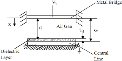
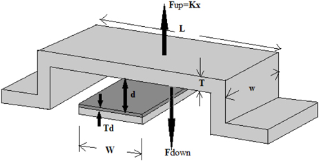
Figure 1 depicts the model of a fixed-fixed MEMS switch with its top and bottom electrodes. The bottom central line is fixed on the substrate and the top one is movable made of either Au or Al [12]. The 3-D view of MEMS shunt switch with geometric dimensions is shown in Fig. 2.
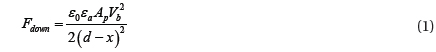
When an actuation voltage is applied between the signal line and the bridge, then electrostatic charges will be induced on both the plates and behave as a parallel plate capacitor. The electrostatic force (Fdown) [13] required to pull down the bridge is given by equation (1).
Where Vb is the applied voltage, x is the displacement and d is the geometric factor, which can be described by equation (2).

Where G is the initial gap between the electrodes, Td is the thickness of the dielectric layer, ε
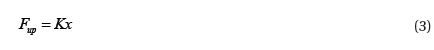
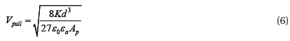
Where K is the spring constant in N/m. At balanced condition, by equating the electrostatic force with the restoring force, the required pull in voltage can be obtained to displace the metal bridge for ‘x’ displacement, which is expressed in equation (4).
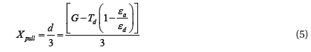
Differentiating equation (4) with respect to x and equating to zero, the critical value of Xpull at which pull in effect occurs is obtained.
Now by substituting equation 5 in 4, the expression for pull-in-voltage at critical value of x is as follows:

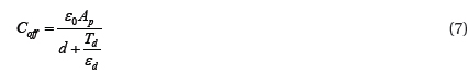
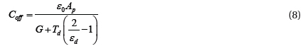
When no actuation voltage is applied between the bridges, then the switch will be in off condition and the value of off state capacitance (Coff) [15] is expressed by equation 7.

Now by substituting equation 2 in 7, the expression for Coff is obtained as follows:
When an actuation voltage is applied, the switch is in on condition and the bridge will come in contact with the dielectric layer. The value of on state capacitance (Con) can be calculated from equation 9 as expressed below:
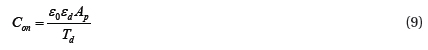
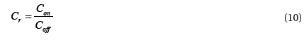
Figure of merit, which is ratio of capacitance of on to off state is given by equation 10.

All the above equations have been validated through the design of a capacitive switch using the standard geometric dimensions by M. Maheswaran et al, as shown in Table 1 and its performance has been analyzed. The different dielectric materials with their dielectric constants used for analysis have been given in Table 2.
[Table 1.] Geometric Dimensions considered for performance analysis of MEMS switch.

Geometric Dimensions considered for performance analysis of MEMS switch.
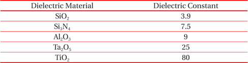
Dielectric materials along with Dielectric Constant values considered for analysis of MEMS switch behavior.
In this paper, five different dielectric layers SiO2, Si3N4, Al2O3, Ta2O5 and TiO2 are considered over the central line of CPW. The variation in pull-in-voltage and capacitance ratio has been predicted for different dielectric layer thickness. Maximum and minimum thickness of dielectric layer is considered from Saucedo-Flores et al. [10]. The effect of variation in dielectric layer thickness on pull-in-voltage and figure of merit for SiO2, Si3N4, Al2O3, Ta2O5 and TiO2 are calculated and shown in Tables 3-7. These Tables describe that with the increase in thickness of the dielectric layer, displacement of the MEMS beam along with pull-in-voltage decreases for different dielectric material. Again, for identical value of dielectric thickness, material with higher dielectric constant provides low actuation voltage, as compared to material with lower dielectric constant. But at 0 μm dielectric thickness, the value of pull in voltage and displacement, of the beam remains same for different dielectric material and figure of merit is infinite, as the value of Con becomes infinite. Theoretical calculation of figure of merit (Cr) is based on equation 10 and dimension of different parameters are described elaborately in Table 1. To get better performance of MEMS switch, these dimensions are standard, as reported in cited references.
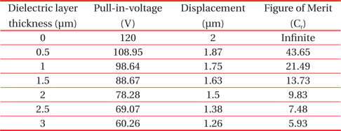
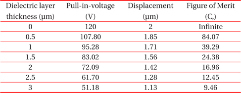
Values of pull-in-voltage, displacement and figure of merit of MEMS switch with dielectric material (SiO2) of different thickness.
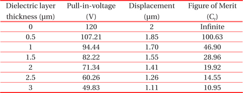
Values of pull-in-voltage, displacement and figure of merit of MEMS switch with dielectric material (Si3N4) of various thicknesses.
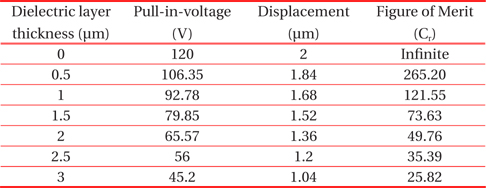
Values of pull-in-voltage, displacement and figure of merit of MEMS switch with dielectric material (Al2O3) of various thicknesses.
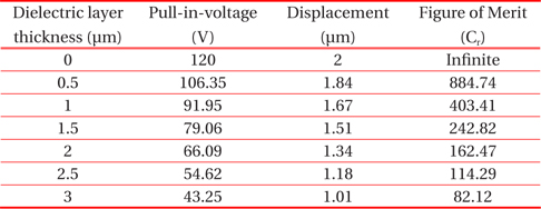
Values of pull-in-voltage, displacement and figure of merit of MEMS switch with dielectric material (Ta2O5) of various thicknesses.
values of pull-in-voltage, displacement and figure of merit of MEMS switch with dielectric material (TiO2) of various thicknesses.
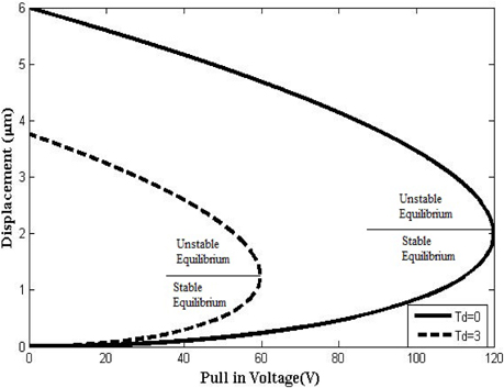
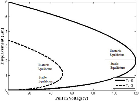
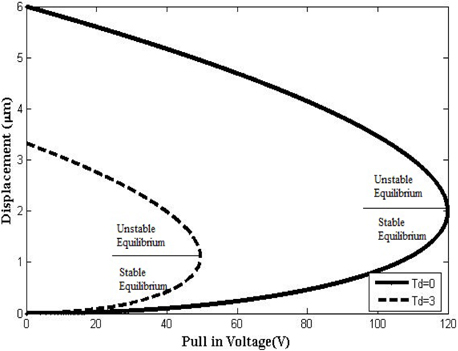
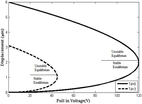
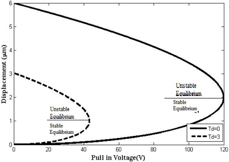
Graphical representation of effect of variation in thickness of dielectric layer on the pull-in-voltage for different dielectric material with and without considering dielectric layer thickness has been shown in Fig. 3 to 7. The straight lines on the curves describe the critical values of displacement at which pull-in effects occur. Above the critical point, the beam is in unstable equilibrium and below this point, the beam attains stable equilibrium. This critical point is derived in equation 5 and graphically represented from Fig. 3 through 7. Above the critical point, the upper branches of curves present negative slope and beam becomes unstable. MATLAB programming was done to represent the effect of dielectric thickness graphically. For every dielectric material, at Td =0 um critical point is (120 V, 2 μm) and above this beam is unstable. Table 8 describes the comparison of decrease in pull-in-voltage in terms of percentage for different dielectric material of dielectric layer thickness 3 μm with reference to thickness 0 μm. The percentage reduction of pull-in-voltage is maximum for SiO2, which is 50% and 35.89% for TiO2, which is the minimum. Therefore, when dielectric layer thickness is increased, pull-in-voltage and displacement parameter is reduced.
[Table 8.] Percentage evaluation of pull-in-voltage for different dielectric material.
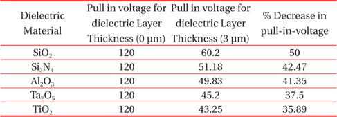
Percentage evaluation of pull-in-voltage for different dielectric material.
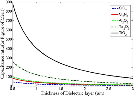
Figure of merit is another performance parameter associated with the switch . The values of figure of merit fall down with increase in thickness of dielectric layer for different dielectric material. For equal values of thickness of dielectric layer, materials with high values of dielectric constants give high figure of merit. Figure 8 is a graphical representation of variation in capacitance ratio for different dielectric material with varying dielectric thickness. The graphical representation has been shown through MATLAB.
This work presented a detailed analysis of effect of dielectric layer thickness in order to reduce the pull-in-voltage and increase the capacitance ratio value using materials such as Silicon Dioxide, Silicon Nitride, Aluminium Oxide, Tantalum Pentoxide and Tatanium Dioxide. The stability of the movable bridge was observed by coupling dielectric layer with the geometric parameter(d) in the equation of pull-in-voltage. For 3 μm SiO2 thickness with reference to 0 μm thickness, maximum percentage reduction (50%) in voltage was observed when compared individually to higher dielectric materials. However, for different materials with identical thicknesses, high dielectric constant materials provide maximum degradation in voltage as well as increase in capacitance ratio in comparison to lower dielectric maerial. Therefore, depending upon the application chosen,the dielectric material with necessary dielectric thickness should be considered. These predicted behaviors of MEMS switch for different dielectric materials will enable researchers and manufacturing companies to design appropriate switch for specific application.