In this study, we proposed a new single-stage small power MH lamp electronic ballast and power-factor correction circuit with improved circuit by the current of passive power factor correction. Main circuit integrates traditional DC/DC and DC/AC circuits into one-stage DC/AC inverter. Moreover, we described the working principle and control strategy of the new circuit; it’s soft switching principle; and resonant element parameter design formula. An experimental prototype of HID lamp electronic ballast with output power of 70 W was built to verify the feasibility of the analysis and design. The simulation and experimental results proved that the power factor of this circuit could reach 94%, with efficiency of 90%. The input current harmonics conform to IEC 61000-3-2 standards and its cost is low. These superior performances of the new circuit indicate certain practical values.
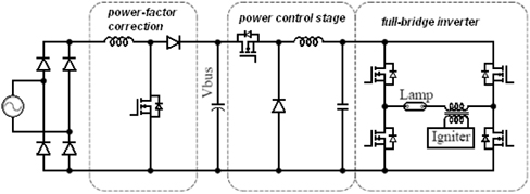
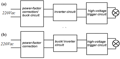
MH lamp is the most representative high intensity discharge (HID) lamp, with good lighting quality, high optical efficiency and energy saving. Thus, it is necessary to have highly steady and reliable electronic ballast. At present, the most typical electronic ballast structure is three-stage, shown as Fig. 1. PFC (power correction circuit) usually adopts Boost circuit; DC/DC adopts Buck circuit; and DC/AC stage adopts half-bridge or full -bridge inverter circuit. With working frequency between 100~400 Hz, low-frequency working state is good for eliminating acoustic resonance [1,2]. Currently, three-stage technology has become more mature. The current total harmonic distortion of this circuit usually is lower than 5%, with power factor close to 1. Because bus voltage is approximately constant, DC/DC stage can be optimized. Moreover, because DC bus voltage is relatively high, a small electrolytic capacitor can be used in certain retention time. However, this scheme needs at least two switch elements and two sets of control circuits, which greatly increases the cost and complexity. In recent years, many researchers change the traditional threestage structure circuit into two-stage circuit in the application of medium-power electronic ballast. The first one is combining PFC with power control circuit and sharing one switching element, also called single-stage PFC circuit [3,4], shown in Fig. 2(a). It integrates PFC with DC/DC and by aid of control technology, one switch can realize two functions, not only guaranteeing power control but also realizing power-factor correction. The second one is combining PFC with DC/AC circuit [5], shown in Fig. 2(b). Full-bridge DC/AC circuit or half-bridge circuit are respectively taken as main circuit and by high and low frequency signals, they jointly work on power switch element and output low-frequency square signals, realizing the control of lamp current and power. In small power electronic ballast, single-stage electronic ballast has been a research hotspot in recent years. With low cost, lamp weight and small volume, single-stage circuit can complete a series of functions of three-stage topological structure and twostage topological structure. Thus, its study is of great reference value. Many literatures have raised single-stage electronic ballast [6-15]. Literature [6] proposed a single-stage electronic ballast circuit and this circuit is the primary circuit integrated by DC/DC and DC/AC and fails to realize PFC function. Added with PFC circuit, this circuit was realized by two-stage circuit. Literature [7] put forward one single-stage electronic ballast circuit, which adopted double-feedback full-bridge BIFRED structure circuit. This circuit completed a series of functions of electronic ballast, for example, PFC, current limiting, and constant power control. In DCM model, Boost-type PFC function can be realized. In inverter driving signals, the joint action of low frequency and high frequency realized low frequency inverter and constant power control. Because of the overly high DC bus voltage in single-stage PFC circuit, bus voltage must be monitored. Some other complex controls (start-up time sequence, current limiting and constant power) limit this scheme. Digital control chip alone can simplify the circuit. Thus, the application range of this circuit is limited.
New single-stage small power MH lamp electronic ballast was proposed in this study. PFC circuit is an improved circuit by the current of passive power factor correction and is simple and convenient, has good performance and needs no control. Main circuit is soft switching full-bridge inverter circuit, which integrates Buck DC/DC converter and full-bridge DC/AC inverter and successfully realizes the combination of DC/DC and DC/AC. With low cost, simple control, high efficiency and good performance, this circuit has been the optimal choice of many small-power electronic ballasts. This paper analyzes the working principle and characteristics of each circuit in detail and makes Pspice simulation on the whole circuit. An experimental prototype of HID lamp electronic ballast with output power of 70 W is built to verify the feasibility of the analysis and design, and the simulation results basically conform to the experimental results.
2. BASIC STRUCTURE OF SINGLE-STAGE ELECTRONIC BALLAST
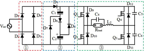
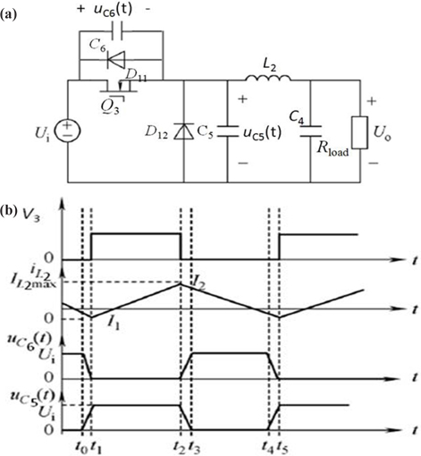
The proposed small-power single-stage electronic ballast topology is shown as Fig. 3. The main circuit is constituted by rectifier circuit (①), circuit by the current of passive power factor correction (②) and inverter circuit with soft switching auxiliary network (③). In ③, Buck DC/DC inverter is integrated with fullstage DC/AC inverter. When switch Q3 and Q4 work at high frequency, it is equivalent to Buck circuit, with regulating function of output power. When Q1 and Q2 work at low frequency, it is equivalent to inverter circuit and outputs low-frequency square signals, which effectively inhibits acoustic resonance. Switch Q3 and Q4 work at 40 KHz, ZVS opening technology are to be adopted. Compared with two-stage circuit, it has simple structure, good reliability and high efficiency.
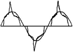
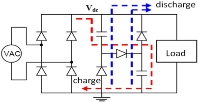
Basic circuit by the current of passive power factor correction is proposed for the electronic ballast for fluorescent lamp. Fig. 4 shows the basic circuit by the current of passive power factor correction and Fig. 5 shows the input side voltage current waveform. The circuit comprises two capacitances and three diodes. A simple passive device is used to replace expensive active device, which greatly reduces the cost and increasing the power factor of ballast to over 90% and reduces current harmonics to 30% below. Its fundamental working is via two series capacitors as filter capacitor and proper equipment with several diodes. In this way, the capacitor is series charged and parallel discharged so as to enhance the conduction angle of rectifier bridge diode and improve the input side power factor.
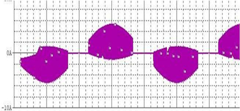
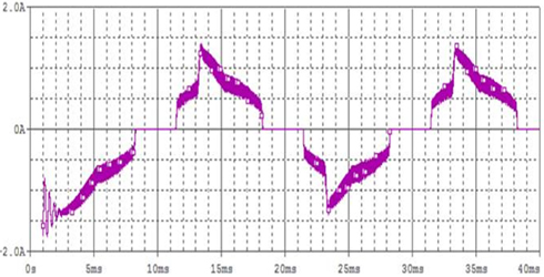
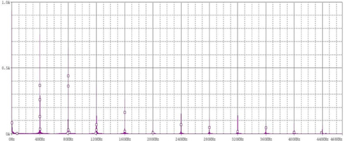
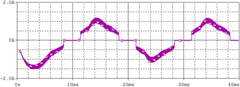
Pspice software is used to simulate the circuit in Fig. 3. The input side current waveform of basic current circuit is detected as a piece of chaotic envelope wave block, shown in Fig. 6. The input side current has numerous high-frequency harmonics. The analysis of FFT inversion spectrogram of input end current indicated that input current contains 40 KHz, 80 KHz and 120 KHz and other 40 KHz related multiple harmonics. This high-frequency harmonics is caused by the disturbance of backward stage highfrequency soft switching inverter, shown in Fig. 7. Thus, future work will include improved current circuit to achieve high power factor and reduce harmonics.
3. IMPROVED SINGLE-STAGE MH LAMP ELECTRONIC BALLAST CIRCUIT
3.1 Improved circuit by the current of passive power factor correction
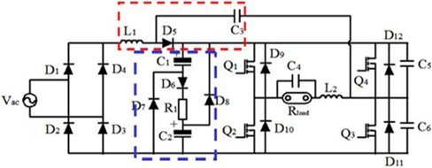
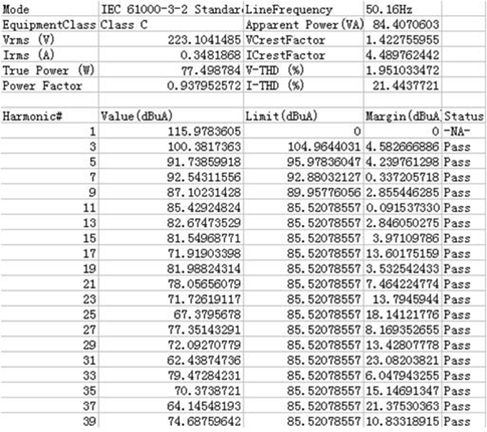
Though basic circuit by the current of passive power factor correction can achieve higher power factor than traditional bridge rectifier capacitor filter circuit, it still has the following problems. (1) Power factor cannot meet the IEC61000-3-2 standards, especially third and fifth harmonic excess. (2) Fig. 6 shows that when input voltage is close to zero point, there is a dead zone of non-input current in the inverter, about 3ms. The existence of dead zone will decrease power factor and generate higher harmonics. Thus, as shown in the improved current circuit in Fig. 8, the new circuit adds inductor L1, capacitor C3 and resistor R1 on the basis of the original circuit, which further improves the power factor and reduces the dead zone of input current.
(1)Adding filter inductor L1
To filter the disturbance of high-frequency soft switching inverter on PFC circuit, filter inductor L1 is added behind the rectifier circuit, constituting LC filter circuit with capacitor in current circuit to filter high-frequency harmonics. As shown in Fig. 8, the improved current circuit consists of filter capacitor C1, C2 and D7, D8, D6 and R1. In each half AC voltage cycle, filter capacitor voltage is charged to AC peak voltage minus three diode voltage (D6 and two diode rectifier bridges). Input current simulation waveform clearly indicates that there is no envelope block in the input side current. The input current FFT inversion spectrogram shows that 40 KHz above high-frequency harmonics has been effectively filtered by filter inductor L1.
(2) Adding steady resistor R1
Input current simulation waveform as in Fig. 9 shows that the peak of the input current is very large. Thus, to limit the peak, steady resistor R1 is added. The input current simulation waveform after adding R1 is shown in Fig. 10. Thus, the peak is effectively controlled and current waveform is smoother.
When AC side input voltage is lower than the voltage at both ends of capacitor C1 and C2, filter capacitor C1, D7 and C2, D8 is paralleled to charge the backward stage and the capacitor voltage at this time is equal to the half of AC voltage peak.

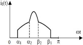
The duration time of capacitor C1 and C2 parallel discharge is 33% of AC input voltage cycle. During (0,α1) and (β1,π) in Fig. 11, if the voltage at both ends of capacitor C1 and C2 remains constant, a1=30°, b1=150°.
During (a1,b1), under no DC/AC stage and directly pure resistance load, the load current is provided by AC input side current.

However, during (a2,b2), the input side current shall be equal to the charge current of capacitor C1 and C2.

Adding capacitor C3 and constituting series resonance tank circuit with L1
To further reduce the time of dead zone, a series resonance tank circuit comprising L1, D5 and C3 is shown in Fig. 8. L1 and quasi resonance capacitor constitute a series resonance tank circuit. Thus, power factor can be improved. After adding resonance tank circuit, the input voltage current simulation waveform is shown as in Fig. 12. Compared with Fig. 10, the output current waveform is closer to sine wave. The working principle is that when Q3 is open, L1 and C3 become series resonance and input current charges C3 by L1 and Q3. When Q3 is turned off, C3 releases charges quickly to reduce the dead zone of input side current and improve the input power factor. The series resonance tank circuit simulation waveform is shown in Fig. 13.
3.2 Soft switch DC/AC inverter
For DC/AC full-bridge inverter constituted of Q1, Q2, Q3 and Q4 in Fig. 8, the topological structure of this circuit is a singlestage soft switching DC/AC circuit, which integrates the common characteristics of Buck DC/DC convertor and full-bridge DC/AC invertor and outputs 50Hz low-frequency square wave. Thus, acoustic resonance can be effectively inhibited. Among them, Q1 and Q2 are low-frequency half-bridge; Q3 and Q4 are high-frequency half-bridge, which determines duty factor. L2, C4, C5 and C6 make up soft switching auxiliary resonance, reducing switching loss of high-frequency Q3 and Q4. In a low-frequency cycle, there are two working stages.
① When Q1 is on, and Q2 is off
When Q1 is on, output DC voltage of circuit by the current of passive power factor correction, Ui transmits energy to load through Q1 and Q3. The energy of inductor L2 increases linearly. At this moment, when Q3 cuts off, inductor L2 releases energy and passes freewheel diode D12. In this stage, inductor L2 releases the increased energy in the former stage to load, keeping the voltage polarity of the load unchanged. Thus, this process is equal to BUCK working mode. Among them, Q3 is master control switch and determines the output voltage and D12 is freewheel diode.
② When Q2 is on, and Q1 is off
When Q2 is on, the working mode is similar to the above stage. The difference is that Q4 is master control switch and D11 is freewheel diode. The output voltage of the load is determined by Q4 and its polarity is contrary to the above stage.
The further analysis of the soft switching principle of fullbridge inverter is shown below. For the convenience of analysis, switch Q3 is taken as research object. In Fig. 8, if the inductor is in critical conduction mode, D12 has no reverse current when Q3 is off but energy saved in C6 may decrease the efficiency of inverter. To overcome this drawback and improve the efficiency of inverter, switch loss is required to be reduced i.e., the ZVS turn-on conditions shall be constructed to realize soft switching. In Fig. 4, if Q3 is on and Q4 is off, suppose DC bus voltage after current circuit is Ui and its equivalent circuit is shown as in Fig. 14a. It is Buck DC/DC converter and its major waveform is shown as 14b. During [0, t0] of t, D12 is on. At t1, current passing through inductor decreases to zero and D12 is turned off. At the same time, L2 and C5 are observed resonance, as well as C6. Thus, during [t0, t1] of t, C6 discharges and uC6 decreases; while at the same time, C5 charges and uC5 increases. At t1, uC6(t)=0, uC5(t)=Ui and VD4 is open. ZVS turn-on condition of Q3 is established and Q3 realizes ZVS turn-on. During [t1, t2]of t, Q3 is on, inductor-current increases. At t2, Q3 is close; L2 and C5 are observed resonance, as well as C6. Thus, uC5 decreases slowly and uC6 increases slowly. Therefore, ZVS conditions of Q3 turn-off exist and Q3 realizes ZVS turn-off. At t3, uC5(t)=0 and uC6(t)=Ui. ZVS conditions of D12 open establish and D12 realizes ZVS turn-on.
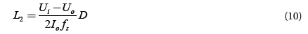
4. PARAMETER DETERMINATION OF RESONANT ELEMENT L2 AND C4 IN MAIN CIRCUIT
When Q3 is on, during t1≤t≤t2=DTs, suppose ΔI=I2-I1 is inductor current peak-peak ripple value, then,
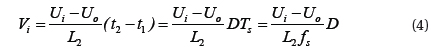
When Q3 is off, during t2≤t≤Ts, inductor-current declines linearly. When t=t5, it declines to I1, then,
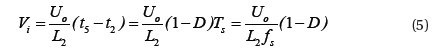
Because iL2(t)=iC4(t)+io(t), it is supposed that the pulse of load current io(t) is extremely small and can be neglected, than ΔiL2=ΔiC4. Moreover, the mean capacitance current in a cycle is zero, the voltage peak-peak ripple value on capacitor can be,
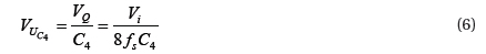
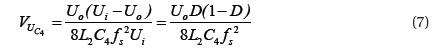
Substituting Formula (4) and Formula (5) into Formula (6), we can express the following,
Further, we can state,

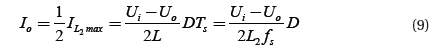
When convertor is in critical conduction mode, the relationship between load current and inductor current can be expressed as,

Thus, L2 can be solved.

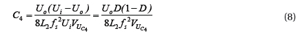
Thus, as long as the design indexes of Io, ΔUC4, fs, Ui, Uo and other parameters are known, L2 and C4 can be determined according to Formula (8) and Formula (10). Resonant capacitor C5 and C6 is capacitor CDS of soft switching at drain-source end. In the actual design, element parameters have dispersity, a pF-stage small capacitor is jointed at the drain-source end of the soft switching for adjustment based on the actual situation. According to experience, it usually is (1/8~1/5)CDS. According to the above determination methods of resonant element parameters, the switch of the experimental prototype is IRFP460, with CDS=750 pF and externally connected with a 100 pF capacitor in parallel. Thus, each resonant parameter is set as, C5=C6=850 pF, C4=0.9 μF and L2=226 μH. The other parameters are L1=300 uH, C3=2.2 nF, R1=10 Ω.
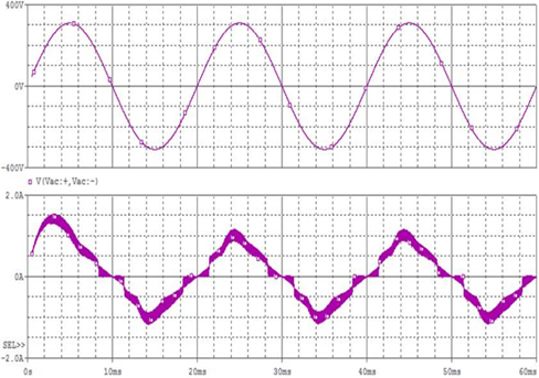
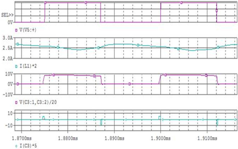
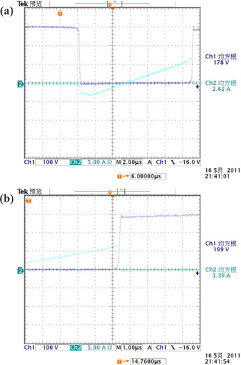
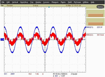
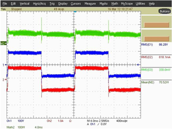
To verify the characteristics of new single-stage electronic ballast, an experimental prototype with output power of 70 W is built. When the experimental prototype works under the load of 70 W MH lamp, the input voltage and current experiment waveform measured in the experiment are shown in Fig. 15 and the odd harmonic simulation analysis of input current is shown in Fig. 16. Thus, current harmonics all conform to IEC61000-3-2 standard. Figure 17 shows Q3 switching process of high-frequency MOS. Hence, Q3 realized soft switching. Figure 18 shows lamp voltage, current and power, where green line represents lamp power; blue line represents lamp voltage; and red line represents lamp current. These measured data and curves indicate that the input current is close to sine wave, with measured power factor of 93.8%. The output end, namely, the end voltage of the lamp, is a low-frequency square signal, so acoustic resonance can be eliminated and MH lamp can work steadily. Moreover, efficiency test is made the experimental prototype, with measured input power of Pin=77.52 W, output power of Pout=70.5 W and efficiency of about 90%.
A new topology fit for small-power MH lamp electronic ballast is proposed; and thorough theoretical analysis, simulation and experimental validation are made on the structure and working principle of the new circuit. The new circuit has the following characteristics.
(1) The new MH lamp single-stage electronic ballast system adopts improved current power correction circuit and main circuit integrates traditional DC/DC and DC/AC circuits into first-stage DC/AC, which makes the circuit simpler and less costly
(2) The new single-stage electronic ballast can be applied to low-power situation, with maximum output power lower than 100W.
(3) The simulation results indicate that the new circuit owns excellent performance, with efficiency of 90%.
(4) Theoretical analysis results demonstrate that the inverter circuit of the new electronic ballast can form ZVS or ZCS conditions when working, which enables inverter switch to work in ZVS or ZCS mode and further greatly reduces the switching loss.
(5) An experimental prototype with output power of 70 W is built to drive MH lamp and the performance results show that the lamp works steadily and strobe and acoustic resonance are eliminated. The experimental results are consistent with the theoretical calculation and simulation results.